

Semiconductor device and manufacturing method therefor
a semiconductor and semiconductor technology, applied in the direction of solid-state devices, coatings, chemical vapor deposition coatings, etc., can solve the problems of short-channel effect of transistors, and achieve the effect of preventing the polysilicon layer from short-circuiting with the wiring materials and preventing the silicon epitaxial layer from short-circuiting
- Summary
- Abstract
- Description
- Claims
- Application Information
AI Technical Summary
Benefits of technology
Problems solved by technology
Method used
Image

Examples
first embodiment
1. First Embodiment
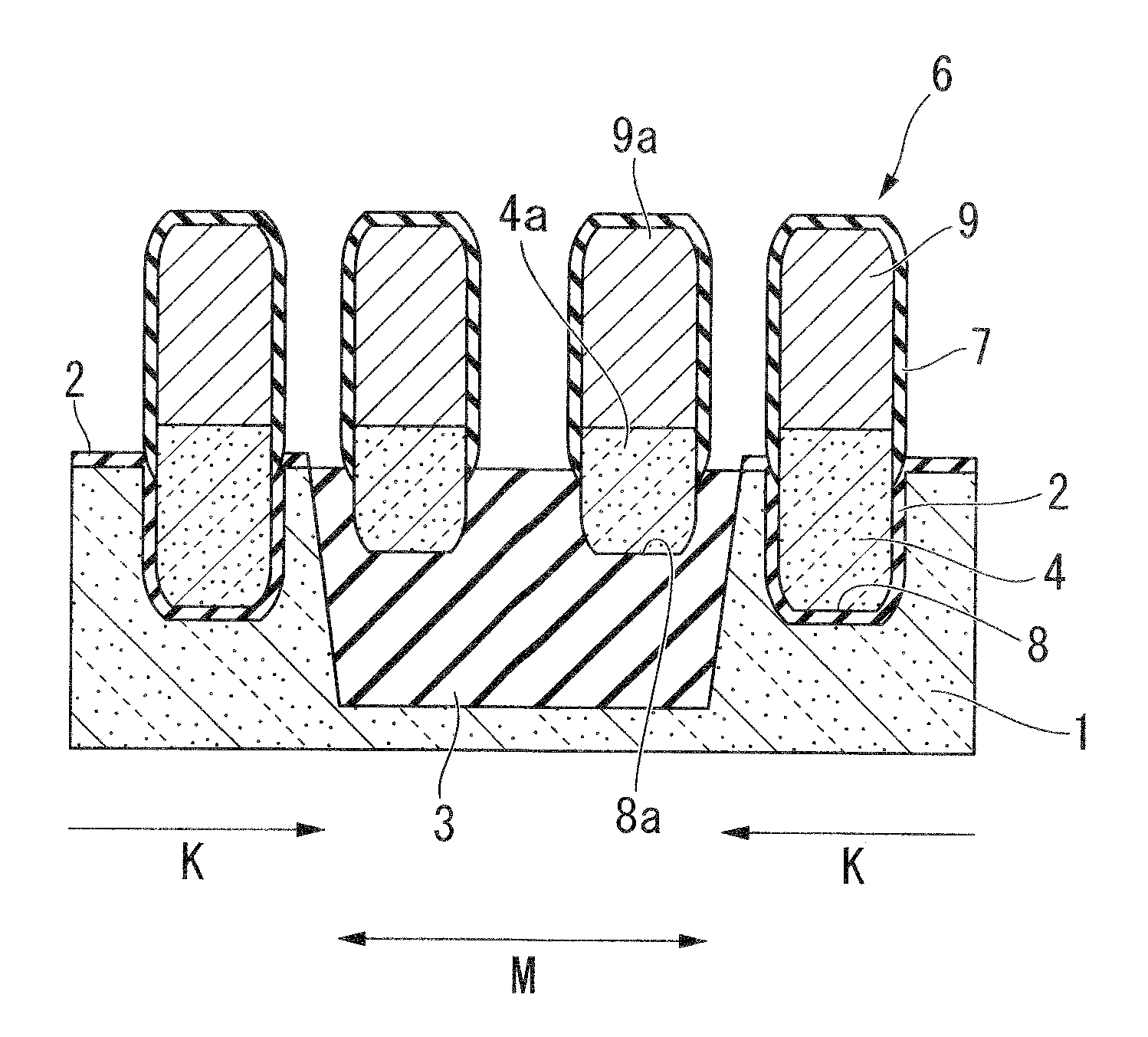
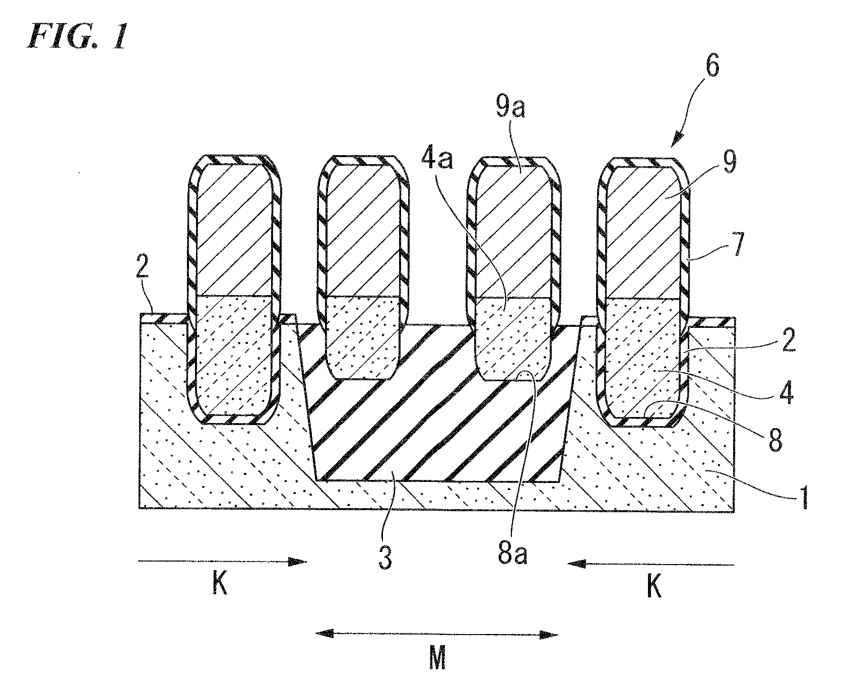
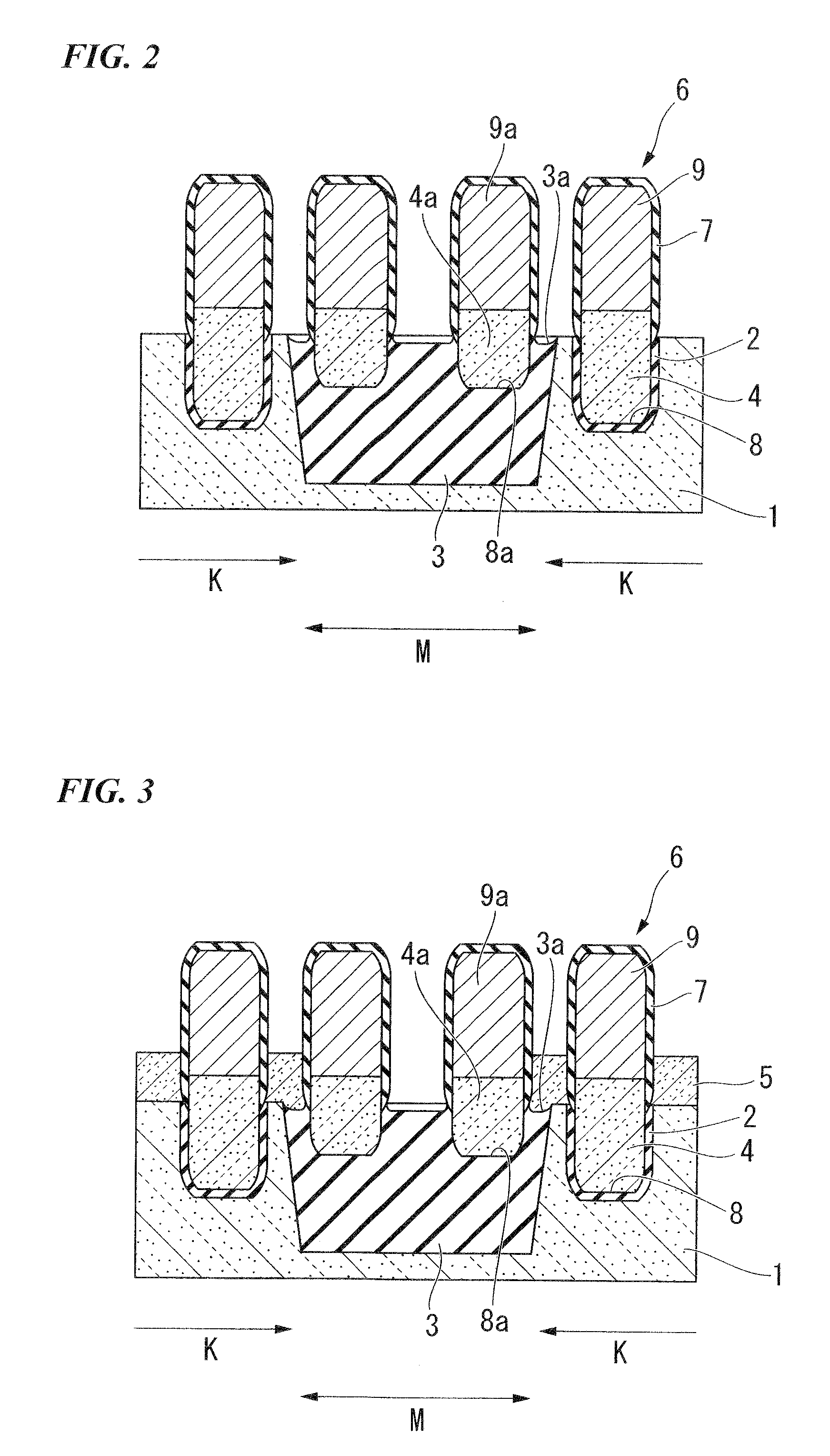
[0054]A first embodiment of the present invention is directed to the manufacturing method of a semiconductor device including an element separation process for forming an STI region and an active region in a silicon substrate, a trench forming process for forming trenches (or channels) in the active region, a gate electrode forming process for forming gate electrodes in trenches, a preprocessing for removing an oxide film via dry etching, and an epitaxial growth process for forming a silicon epitaxial layer via selective epitaxial growth. The details of the processes will be described with reference to FIGS. 1 to 3.
(a) Element Separation Process
[0055]As shown in FIG. 1, an STI element separation region (hereinafter, simply referred to as an element separation region) M is formed on the silicon substrate 1 in accordance with the STI (i.e. Shallow Trench Isolation) method. The element separation region M corresponds to an embedded insulating film 3 (composed of sili...
second embodiment
2. Second Embodiment
[0071]A second embodiment of the present invention will be described with reference to FIGS. 4 to 6.
[0072]The second embodiment is directed to preprocessing which is performed before the formation of contact plugs disposed in semiconductor devices.
[0073]FIG. 4 shows that contact holes are formed in a metal-oxide semiconductor (MOS) transistor formed on a silicon substrate 210, wherein source / drain regions 202 are formed on both sides of a gate electrode 201, and an interlayer insulating film 203 is formed on the entire surface via CVD. As the interlayer insulating film 203, it is possible to use an HDP-CVD film as well as other silicon oxide films, which are formed via low-pressure CVD causing thermal reaction between dichloro-silane or mono-silane (SiH4) and dinitrogen monoxide (N2O) at high temperature and low pressure conditions, via normal-pressure CVD causing reaction between mono-silane and oxygen at a low-temperature condition, via plasma CVD using an appa...
third embodiment
3. Third Embodiment
[0088]A manufacturing method of a semiconductor device according to a third embodiment of the present invention will be described with reference to FIGS. 12 and 13, which are used to explain a preprocessing in a crown capacitor fabrication process.
[0089]In FIG. 12, metal plugs 406 connected with wires 408 are embedded in a first interlayer insulating film 407, the surface of which is covered with an etching stopper layer 405 composed of nitrogen. A second interlayer insulating film 404 is formed on the surface of the first interlayer insulating film 407.
[0090]Recesses are formed in the second interlayer insulating film 404; then, lower electrodes 402 having cylindrical shapes are formed to coat the interior surfaces and the bottoms of the recess, wherein bottoms 402a thereof are brought into contact with the wires 408.
[0091]By way of photolithography, a bridged nitride film 403 having a prescribed pattern is formed on the surface of the second interlayer insulatin...
PUM
| Property | Measurement | Unit |
|---|---|---|
| temperature | aaaaa | aaaaa |
| temperature | aaaaa | aaaaa |
| temperature | aaaaa | aaaaa |
Abstract
Description
Claims
Application Information