Semiconductor Photodiode And Method Of Manufacture Thereof

a technology of semiconductors and photodiodes, applied in the field of semiconductor photodiodes, can solve the problems of telcordia aging test, photodiode characteristics to drift with time, and other problems, and achieve the effect of reducing the number of manufacturing steps, high gain-bandwidth product parameters, and high reliability standards

Active Publication Date: 2009-10-01
LUMENTUM OPERATIONS LLC
View PDF24 Cites 31 Cited by
  • Summary
  • Abstract
  • Description
  • Claims
  • Application Information

AI Technical Summary

Benefits of technology

[0018]It is an object of the present invention to provide a semiconductor photodiode which has a high gain-bandwidth product parameter and which meets high reliability standards of opt

Problems solved by technology

Even though effort has been invested in the development of surface-passivation techniques intended to reduce the surface defects and traps, nonetheless, many photodetector types, mesa-based photodetectors in particular, have not yet been able to deliver satisfactory performance to pass stringent Telcordia aging tests.
Device modeling shows the electric field within these layers remains at a very high value and extends further away from the photon detection area, which can cause photodiode characteristics to drift with time.
Unfortunately, increasing electric field can cause another problem to occur.
Unwanted fringe electric fields often appear at the edges of electrode(s) of the photodiode, which may lead to an uncontrollable, ong

Method used


Image

  • Semiconductor Photodiode And Method Of Manufacture Thereof
  • Semiconductor Photodiode And Method Of Manufacture Thereof
  • Semiconductor Photodiode And Method Of Manufacture Thereof

Examples


Embodiment Construction

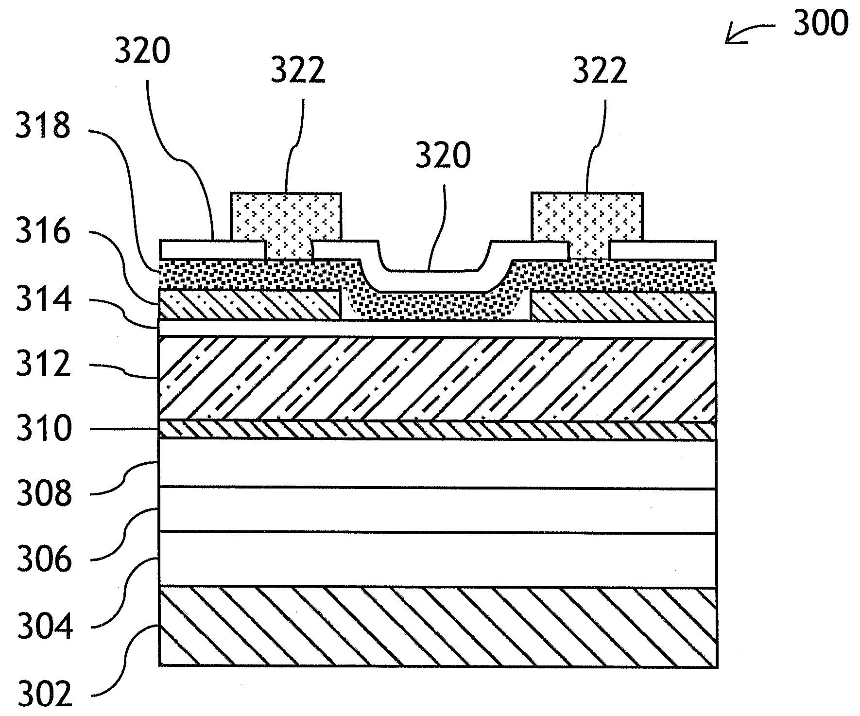
[0040]While the present teachings are described in conjunction with various embodiments and examples, it is not intended that the present teachings be limited to such embodiments. On the contrary, the present teachings encompass various alternatives, modifications and equivalents, as will be appreciated by those of skill in the art. Also, it should be understood that the individual steps of the methods of the present invention can be performed in any order and / or simultaneously, for as long as the invention remains operable.

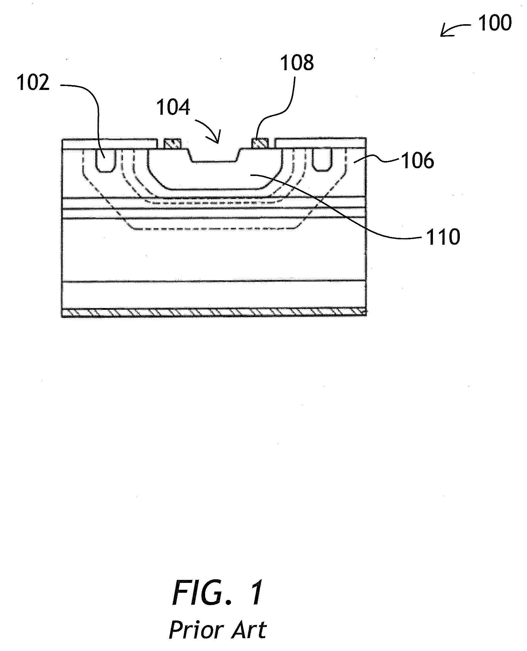
[0041]Referring now to FIG. 1, a prior art avalanche photodiode 100 having a floating protection ring 102 and a concave portion 104 in the multiplying layer 106, is shown. Double-step dopant diffusion with two intermediate photolithographic mask formation steps is necessary to create the dopant pattern including central area 110 and the protection ring 102. The p-type ohmic metal layer 108 is located in a photosensitive area of the avalanche photodiode 100 limiti...


PUM


Abstract

A method of manufacture of an avalanche photodiode involving a step of making a recess in a top window layer of an avalanche photodiode layer stack, such that a wall surrounding the recess runs smoothly and gradually from the level of the recess to the level of the window layer. Further, diffusing a dopant over the entire window layer area so as to form a p-n junction at the bottom of the recess, and providing a first electrical isolation region around the recess by buried ion implantation or wet oxidation in order to limit the flow of electrical current to the p-n junction. Forming an isolation trench around the photodiode and a second electrical isolation region by ion implantation into the trench such that the second electrical isolation region runs through the absorption layer of the photodiode.

Description

TECHNICAL FIELD[0001]The present invention is related to semiconductor photodiodes such as positive-intrinsic-negative (p-i-n) or avalanche photodiodes, and in particular, to InAlAs / InGaAs avalanche photodiodes.BACKGROUND OF THE INVENTION[0002]In optical communication systems, photodetectors are used to convert optical signals into electrical signals. The most commonly used photodetectors are positive-intrinsic-negative (p-i-n) photodiodes and avalanche photodiodes.[0003]A typical p-i-n photodiode includes an absorption layer of intrinsic, i.e. not intentionally doped, semiconductor material between a region of extrinsic, i.e. doped, semiconductor material of a first conductivity type, i.e. n-type or p-type, and a region of extrinsic semiconductor material of a second conductivity type, i.e. p-type or n-type, an arrangement that produces an electric field in the absorption layer. In operation in photoconductive mode, a reverse voltage is applied to the p-i-n photodiode to enhance th...

Claims


Application Information

Patent Timeline
IPC IPC(8): H01L31/0336H01L31/18
CPCH01L31/107Y02E10/544H01L31/1844H01L31/1075
Inventor HU, SYN-YEMPAN, ZHONG
Owner LUMENTUM OPERATIONS LLC
Why Eureka
Try Eureka