Analog-to-digital converter
a converter and analog technology, applied in the field of analog-to-digital converters, can solve the problems of significant power consumption of the sub-adcs comparator relative to the residue amplifier, and achieve the effect of reducing power consumption
- Summary
- Abstract
- Description
- Claims
- Application Information
AI Technical Summary
Benefits of technology
Problems solved by technology
Method used
Image
Examples
Embodiment Construction
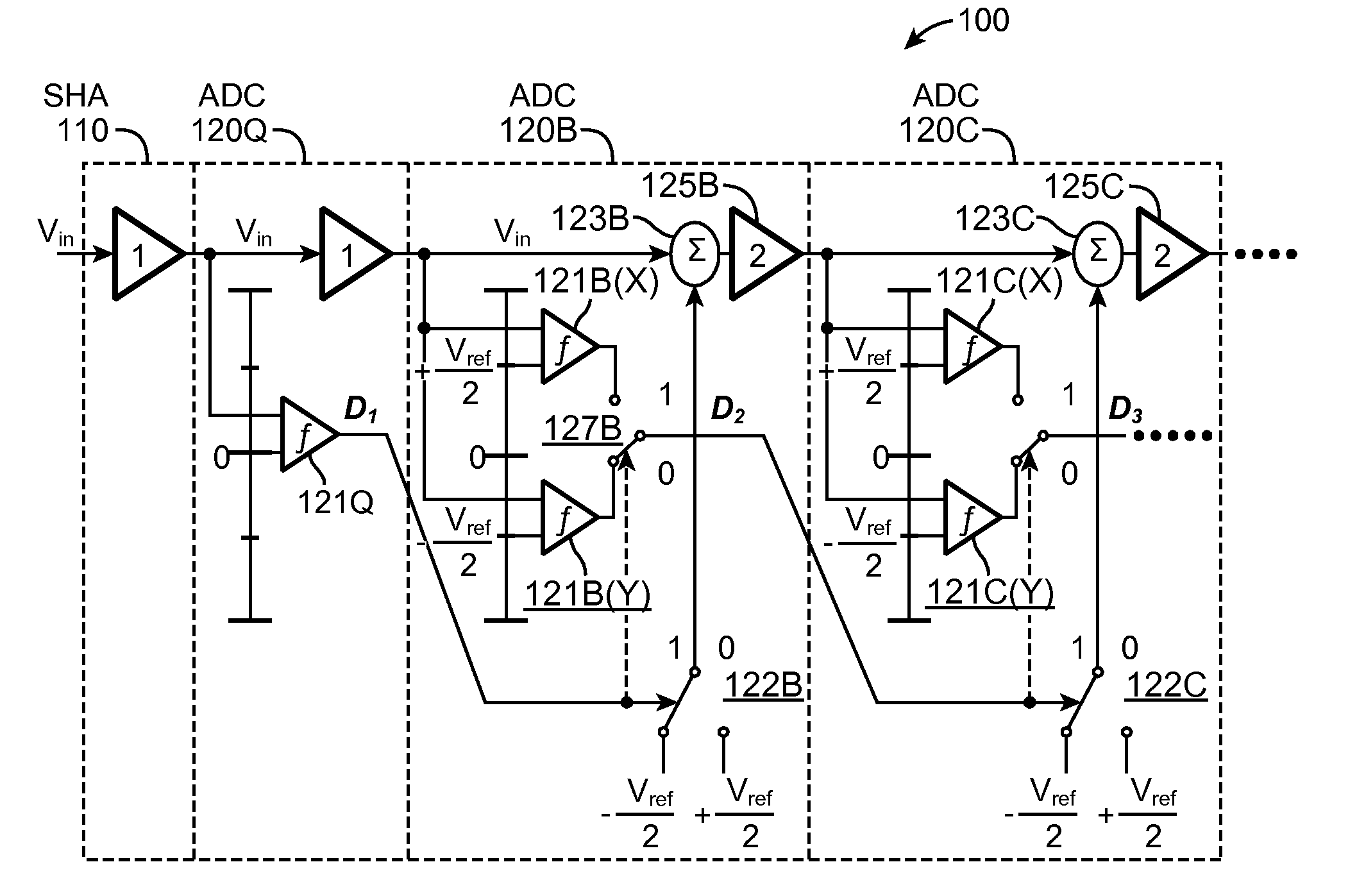
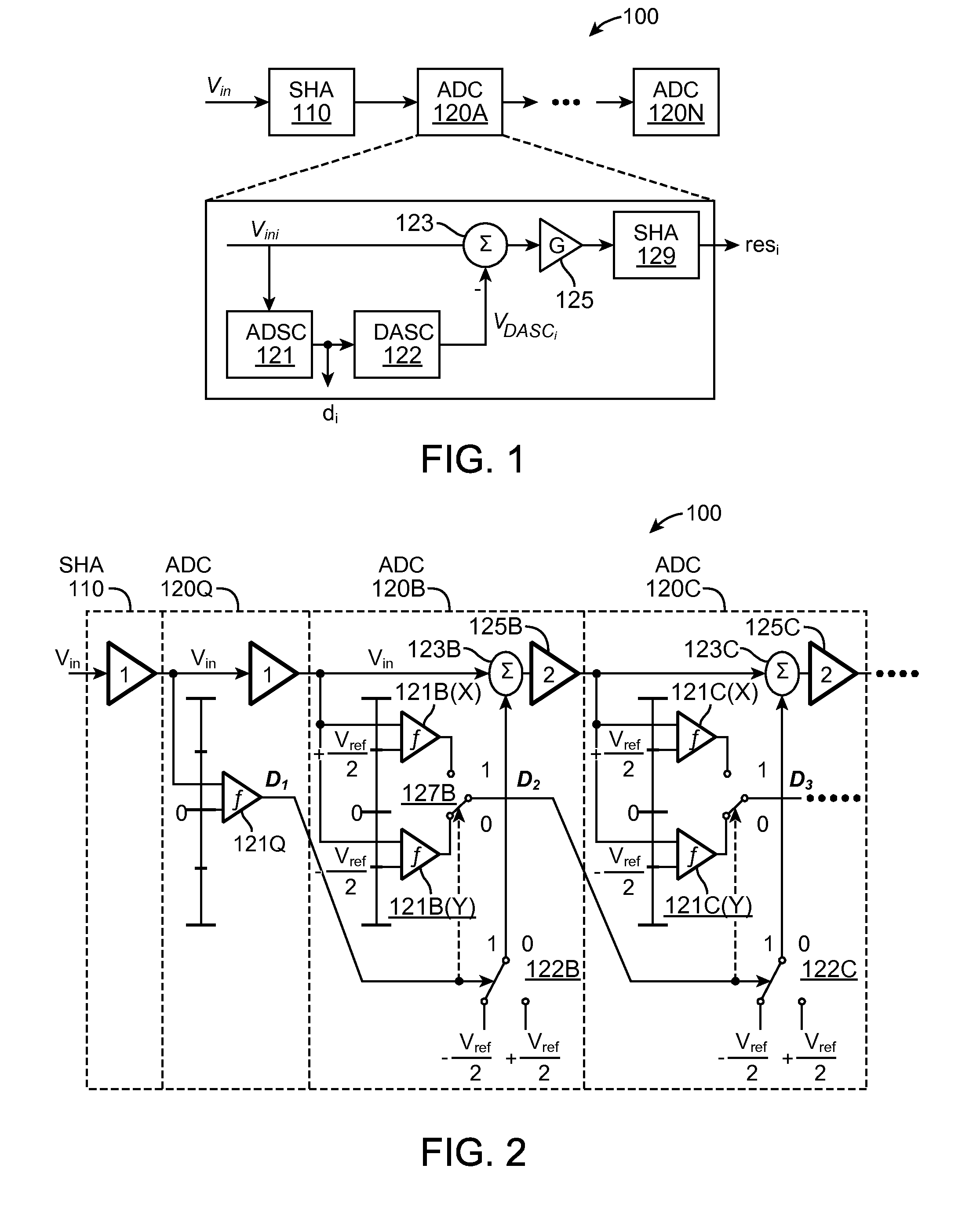
[0030]Throughout the following description, a 10.3 GS / s 6 bit ADC with an input bandwidth of 5.1 GHz will be used to illustrate various aspects of the invention. To increase resolution with moderate power dissipation, this example circuit uses a pipelined architecture with open-loop amplifiers and digital calibration. Various trimming circuits are used to enhance yield over process. A 1 bit per stage approach increases the gain-bandwidth product for a given power consumption. To achieve a bit error rate (BER)−12 required by the example application (90 nm CMOS MLSD MMF transceiver), each comparator utilizes a probability of a meta-stable event significantly lower than 10−12, resulting in a comparator maximum clock rate of 1.5 GHz. An 8 way interleaved ADC design is used, comprising 8 ADC channels clocked at 1.3 GHz. Each ADC channel includes two ADC pipelines, allowing continuous background calibration. The input of each pair is selected through an analog multiplexer. In a convention...
PUM
 Abstract
Description
Claims
Application Information


