Eureka AIR delivers breakthrough ideas for toughest innovation challenges, trusted by R&D personnel around the world.

Analyzing device for circuit device, circuit device analyzing method, analyzing program, and electronic medium

Inactive Publication Date: 2009-10-01
PANASONIC CORP
View PDF15 Cites 4 Cited by
  • Summary
  • Abstract
  • Description
  • Claims
  • Application Information

AI Technical Summary

Benefits of technology

[0014]The invention is contrived in view of the above-mentioned situations. An advantage of the invention is to provide an electromagnetic field analyzing method of a circuit device, which can greatly reduce the analyzing time while maintaining the necessary analysis precision.
[0015]According to an aspect of the invention, there is provided an analyzing device for a circuit device including: a computing unit which computes a coupling state between elements of the circuit device; a memory unit connected to the computing unit; and an input unit connected to the computing unit. Here, the computing unit includes a division section dividing the circuit device into a plurality of areas on the basis of layout data of the circuit device, and a coupling ignoring section performing a setting operation of ignoring a coupling between the areas divided by the division section.
[0016]In the analyzing device, the computing unit may include a coupling specifying section (a) specifying a coupling occurrence position in the layout of the circuit device, and a coupling ignoring section (b) performing the setting operation of ignoring the coupling in the coupling occurrence position.
[0017]In the analyzing device, the division section may divide a wiring area of the circuit device into meshes and give a determinant to the meshes to form a determinant, and the coupling ignoring section (b) may replace at least a part of off-diagonal elements of the determinant with 0.
[0018]In the analyzing device, the coupling ignoring section (b) may have a function of setting a coupling ignoring range on the basis of the minimum distance.
[0019]In the analyzing device, the coupling specifying section (a) may have a function of displaying mutual inductance and capacitance as circuit constants at a layout level.

Problems solved by technology

However, to compute the amount of inter-wiring interference, it is required to calculate characteristics of the wirings using complex computations based on the electromagnetic field analysis.
Accordingly, unlike the analysis of a simple textbook wiring model, it is often difficult to consider the amount of inter-wiring interference in actually designing complex wirings.
It is often impossible to make the computation within the finite operating time.
Therefore, the consideration of the amount of inter-wiring interference often depends on an expert designer's sense, not the electromagnetic field analysis, or often depends on trial and error without considering the amount of inter-wiring interference.

Method used


Image

  • Analyzing device for circuit device, circuit device analyzing method, analyzing program, and electronic medium
  • Analyzing device for circuit device, circuit device analyzing method, analyzing program, and electronic medium
  • Analyzing device for circuit device, circuit device analyzing method, analyzing program, and electronic medium

Examples


Embodiment Construction

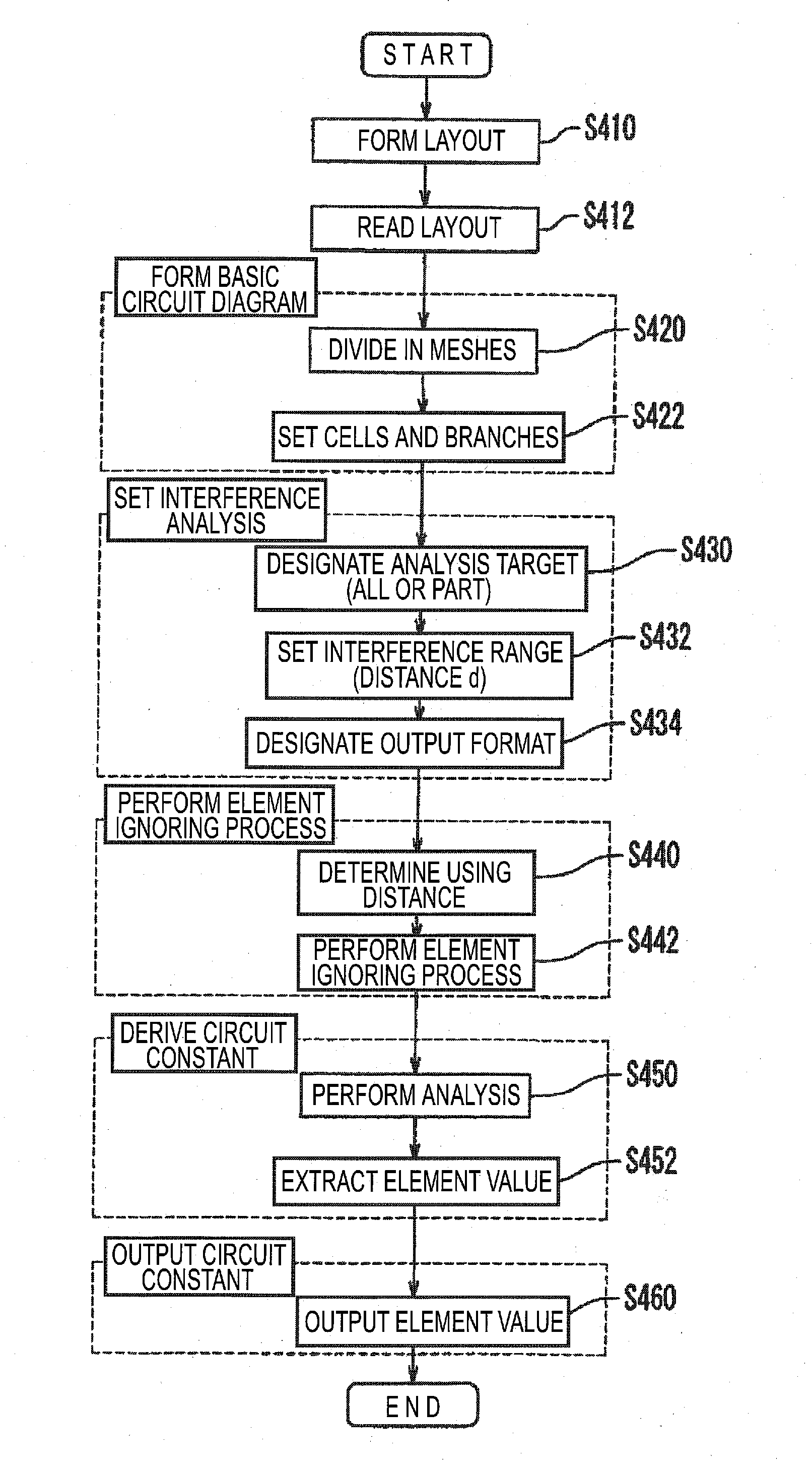
[0095]Hereinafter, embodiments of the invention will be described with reference to the accompanying drawings. In the following drawings, elements having substantially like functions are referenced by like reference numerals for the purpose of brief explanation. The invention is not limited to the following embodiments.

[0096]The inventor knew that the processing time is great as the result of verification of inter-wiring interference in a complex wiring pattern using an electromagnetic field analysis, but it is possible to make a computation in selective consideration of coupling elements (such as parasitic capacitor C) greatly contributing to the inter-wiring interference and thus to greatly reduce the analyzing time without damaging the analysis precision, when interactions (coupling occurrence positions) between individual cells can be specified in advance before performing the electromagnetic field analysis. The invention is based on the knowledge. Hereinafter, the knowledge wil...


PUM


Abstract

A circuit board analyzing method and a circuit board analyzer are provided which can greatly reduce analyzing time. The circuit board analyzer includes a computing unit 110, a memory unit 140 connected to the computing unit 110, and an input unit 160 connected to the computing unit 110. The computing unit 110 includes a wiring data acquiring section 310 acquiring data of wirings formed on a circuit board, a basic circuit diagram forming section 320 dividing the wirings into meshes and setting cells and branches connecting the adjacent cells, and an interference analysis setting section 330 setting an element ignoring range of elements set in the cells and the branches.

Description

TECHNICAL FIELD[0001]The present invention relates to an analyzing device for a circuit device, a circuit device analyzing method, an analyzing program, and an electronic medium, and more particularly, to a method of analyzing an electromagnetic field of a circuit device used in various electronic apparatuses.BACKGROUND ART[0002]The design of a printed circuit board (wiring board) is often carried out by the use of a printed circuit board CAD (Computer Aided Design) device using a computer (for example, Patent Document 1). Many portions of the design of a printed circuit board using a CAD device are automated, but the appropriate design thereof can often be carried out by only an expert designer.[0003]In design of a printed circuit board of a high-frequency circuit, inter-wiring interference often has a great influence on a transmission characteristic. However, to compute the amount of inter-wiring interference, it is required to calculate characteristics of the wirings using comple...

Claims


Application Information

Patent Timeline
IPC IPC(8): G06F17/50
CPCG06F17/5018H05K3/0005G06F17/5036G06F30/23G06F30/367H05K3/00
Inventor URIU, KAZUHIDEYAMADA, TORUYAMAOKA, MASAHIRO
Owner PANASONIC CORP
Why Eureka
Eureka Blog
Learn More