Solid-state imaging device, signal processing method of solid-state imaging device, and electronic apparatus

Active Publication Date: 2009-10-08
SONY CORP
View PDF2 Cites 44 Cited by
  • Summary
  • Abstract
  • Description
  • Claims
  • Application Information

AI Technical Summary

Benefits of technology

[0016]The plurality of rectangular unit pixels are combined to form a square pixel, and the plurality of signals read out from the plurality of unit pixels are output as a single signal. Thereby, the single signal can be handled as the signal from a square grid (a square pixel). If incident light is sampled at spatially equal intervals in the vertical and horizontal directions, it is possible to make the plurality of unit pixels look like a square grid. With the single signal handled as the signal from a square grid, it is unnecessary to change the configuration of a signal processing system at a subsequent stage. Further, if the single signal is selected as necessary from or synthesized from the respective signals of the plurality of unit pixels, it is possible to perform a process of improving the imaging characteristic, such as a process of increasing the dynam

Problems solved by technology

If the pixel pitch becomes less than the resolution of a lens, however, the resolution is not increased.
Even at F4, it is

Method used


Image

  • Solid-state imaging device, signal processing method of solid-state imaging device, and electronic apparatus
  • Solid-state imaging device, signal processing method of solid-state imaging device, and electronic apparatus
  • Solid-state imaging device, signal processing method of solid-state imaging device, and electronic apparatus

Examples


first embodiment

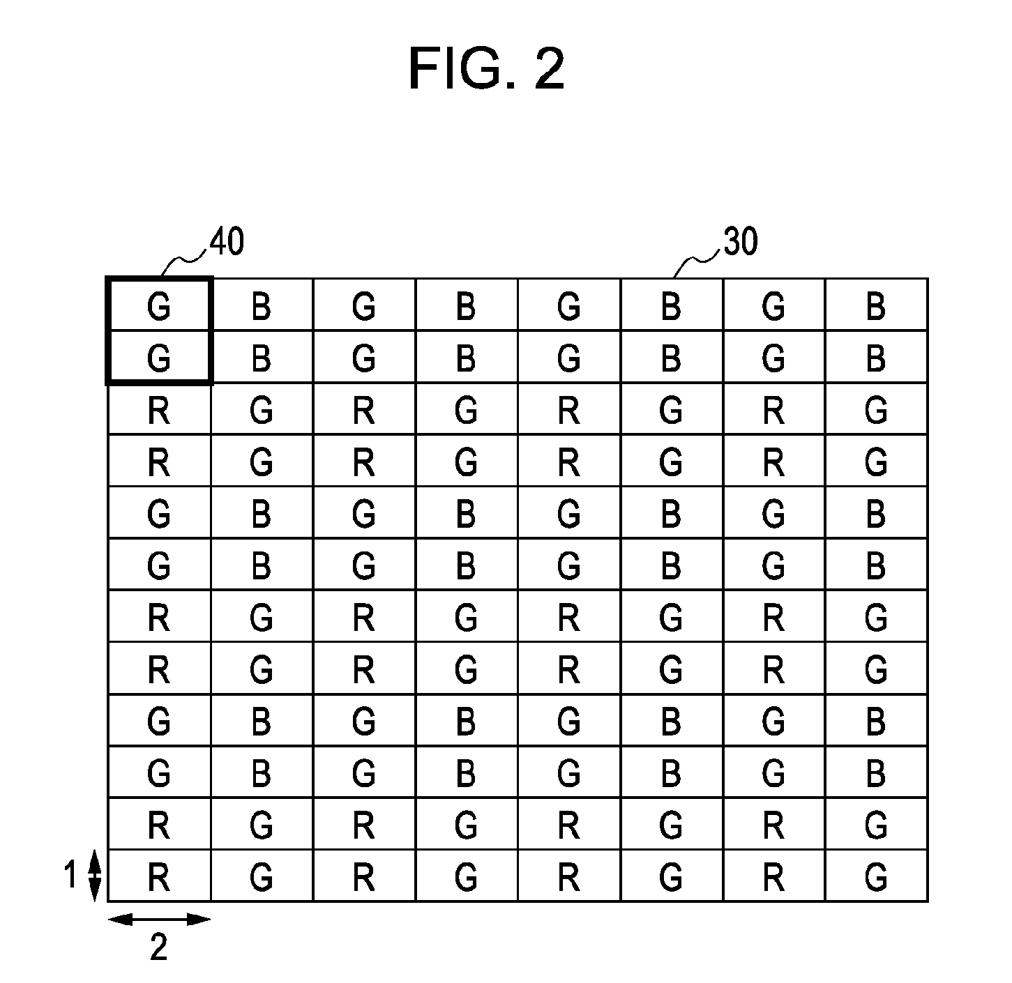
[0055]FIG. 2 is a configuration diagram illustrating an example of the pixel array in the pixel array section 12 according to the first embodiment. As illustrated in FIG. 2, the pixel array section 12 includes unit pixels 30 each including a photoelectric conversion element and two-dimensionally arranged in multiple rows and columns. Herein, each of the unit pixels 30 is a so-called horizontally long rectangular pixel, which is twice as long in the horizontal size (in the row direction) as in the vertical size (in the column direction), i.e., which has a vertical-to-horizontal pitch ratio of 1:2.

[0056]If the CMOS image sensor 10 according to the present embodiment is capable of picking up a color image, color filters, e.g., on-chip color filters 40, are provided on respective light receiving surfaces of the unit pixels 30. Herein, a plurality, e.g., two of the unit pixels 30 adjacent in the vertical direction form a set. The set of two upper and lower pixels is provided with an on-c...

first modified example

[0091]To address the issue of collection of light by using the on-chip lenses, it is preferable to employ, as a back-surface incident type pixel structure or a photoelectric conversion film lamination type pixel structure, a pixel structure having an aperture ratio of 100% and not using the on-chip lenses. The back-surface incident type pixel structure receives incident light from the opposite side to a wiring layer. The photoelectric conversion film lamination type pixel structure performs photoelectric conversion at a photoelectric conversion film laminated on the incident light side of a wiring layer. An example of the back-surface incident type pixel structure will be described below.

[0092]FIG. 6 is a cross-sectional view illustrating an example of the back-surface incident type pixel structure. Herein, a cross-sectional structure of two pixels is illustrated.

[0093]In FIG. 6, photodiodes 42 and pixel transistors 43 are formed in a silicon portion 41. That is, the silicon portion...

second modified example

[0097]In the above-described first embodiment, the shutter scanning is performed separately on the odd row and the even row to cause a difference in the accumulation time and thus provide the two upper and lower pixels with different sensitivities. Alternatively, another method of providing different sensitivities may be employed. For example, ND (Neutral Density) filters may be pasted only on the even rows, or on-chip lenses 49 may be provided only to the unit pixels 30 in the odd rows, as illustrated in FIG. 7. With this structure, the two upper and lower pixels can have different sensitivities. Herein, the ND filter refers to a light amount adjusting filter which substantially uniformly reduces the amount of visible-range light without affecting the color.


PUM


Abstract

A solid-state imaging device includes a pixel array section and a signal processing section. The pixel array section is configured to include a plurality of arranged unit pixels, each of which is a rectangular pixel having different sizes in the vertical and horizontal directions, and a plurality of adjacent ones of which are combined to form a square pixel having the same size in the vertical and horizontal directions. The signal processing section is configured to process a plurality of signals read out from the combined plurality of unit pixels and to output the processed signals as a single signal.

Description

BACKGROUND OF THE INVENTION[0001]1. Field of the Invention[0002]The present invention relates to a solid-state imaging device, a signal processing method of a solid-state imaging device, and an electronic apparatus.[0003]2. Description of the Related Art[0004]In a solid-state imaging device, such as a CCD (Charge Coupled Device) image sensor and a CMOS (Complementary Metal-Oxide Semiconductor) image sensor, unit pixels are in many cases arranged in a grid-like pattern at a predetermined pitch in the vertical and horizontal directions (see Japanese Unexamined Patent Application Publication No. 2007-189085, for example).[0005]A pixel array having the same pitch in the vertical and horizontal directions is easy to be signal-processed, and thus has become a mainstream these days. Pixels arranged at the same pitch in the vertical and horizontal directions, i.e., pixels each having the same size in the vertical and horizontal directions are called square pixels. Meanwhile, pixels arranged...

Claims


Application Information

Patent Timeline
IPC IPC(8): H04N5/228H04N5/335H01L27/146H04N5/355H04N5/369H04N5/374H04N5/378
CPCH01L27/14621H01L27/14625H01L27/14643H01L27/14641H04N5/35563H01L27/1464H04N5/23229H01L27/14627H01L27/14607H04N23/80H04N25/585H04N25/713H04N25/75H04N25/65H04N25/67H04N25/616H04N25/745H04N25/767
Inventor MABUCHI, KEIJI
Owner SONY CORP
Why Eureka
Try Eureka