Semiconductor device and method of fabrication

a semiconductor and semiconductor technology, applied in the direction of semiconductor devices, electrical devices, transistors, etc., can solve the problems of difficult to obtain the desired shallow and low-resistant diffusion layer, excess point defects are often generated, and the desired impurity profile cannot be obtained in the p-type extension diffusion layer, etc., to achieve the effect of improving the drive capability of the transistor, reducing the resistance, and high drive capability

Active Publication Date: 2009-11-12
TAIWAN SEMICON MFG CO LTD
View PDF11 Cites 22 Cited by
  • Summary
  • Abstract
  • Description
  • Claims
  • Application Information

AI Technical Summary

Benefits of technology

[0046]As described above, according to the semiconductor device of the present disclosure and the method of fabrication thereof, an extension diffusion layer having a shallower junction and a lower resistance that is required for further miniaturization can be achieved, and a miniature device having high drive capability can be obtained. Also, extension diffusion layers can be easily caused to have asymmetric impurity profiles. For example, by performing co-implantation with respect to only one (e.g., a source region) of source and drain regions, the source region is caused to have a shallow and steep impurity profile, so that the concentration gradient of carriers between the source region and a channel region can be caused to large. As a result, the drive capability of the transistor can be improved. Also, in this case, the drain region has an impurity profile deeper than that of the source region, so that the occurrence of hot carriers can be suppressed.

Problems solved by technology

Therefore, in this case, there is a problem that a desired impurity profile cannot be obtained in the P-type extension diffusion layer 7.
Excess point defects are often generated mainly by implantation damage during ion implantation.
Even if the implantation energy of ion implantation is reduced so as to obtain a shallower junction, the TED of an implanted dopant becomes significant, which makes it difficult to obtain a desired shallow and low-resistant diffusion layer only by implantation of a single element with low energy.
On the other hand, if fluorine is implanted into the gate electrode 5 and the gate insulating film 4, boron is diffused from the gate electrode 5 to the N-type channel diffusion layer 3, and moreover, the gate insulating film 4 has variations in film thickness, leading to a deterioration in reliability.
However, the reduction of the fluorine dose decreases the suppression effect of fluorine on the TED of boron.

Method used


Image

  • Semiconductor device and method of fabrication
  • Semiconductor device and method of fabrication
  • Semiconductor device and method of fabrication

Examples


first embodiment

Variation of First Embodiment

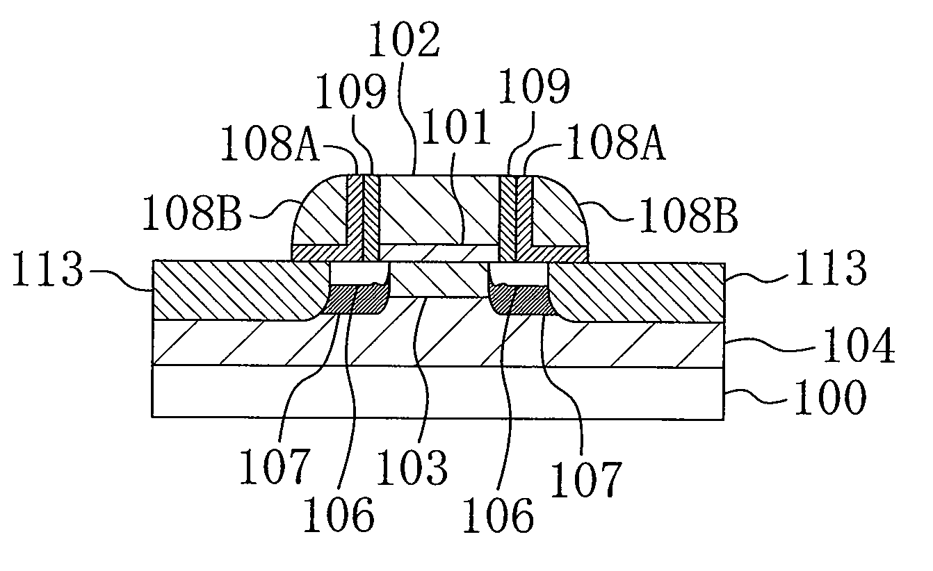
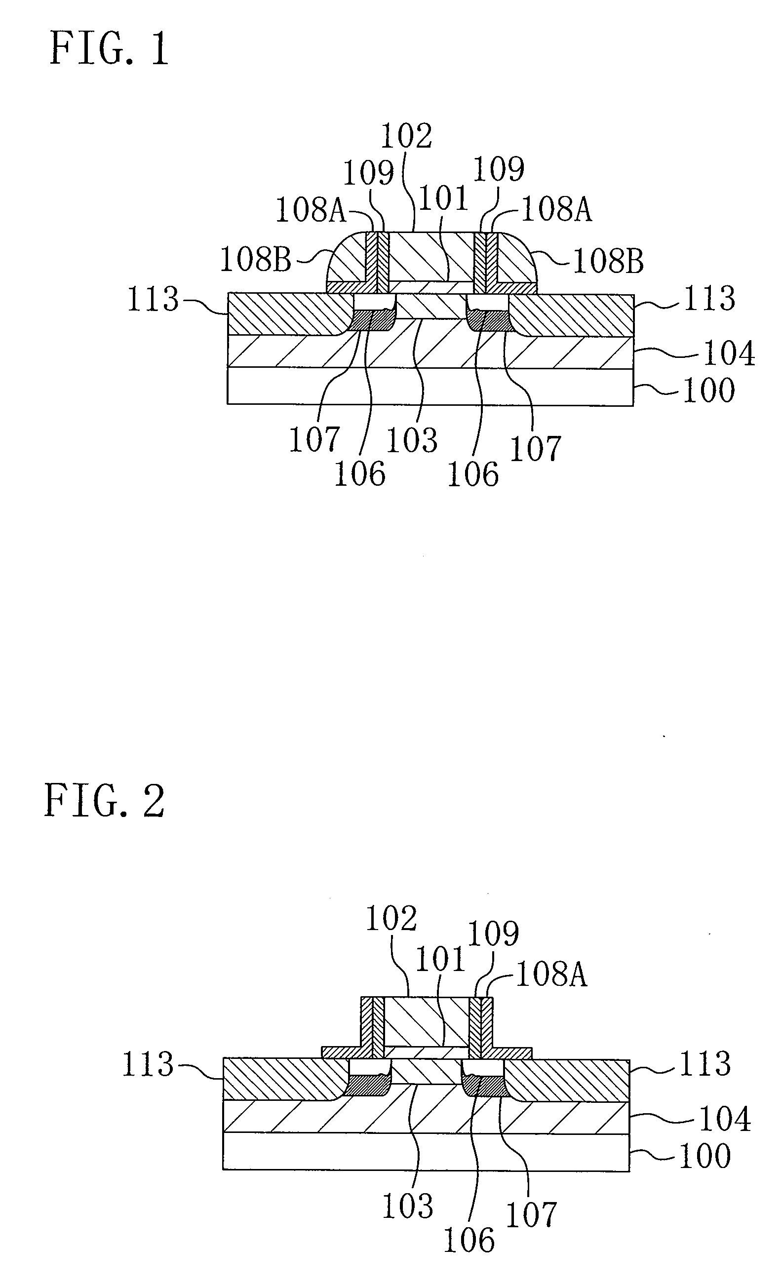
[0072]FIG. 2 is a cross-sectional view showing a structure of a semiconductor device according to a variation of the first illustrative embodiment. As shown in FIG. 2, in the semiconductor device of this variation, first sidewalls 108A and second sidewalls 108B contain fluorine, while P-type source and drain diffusion layers 113 contain fluorine (F) and carbon (C).

[0073]Also, in the semiconductor device of this variation, the second sidewalls 108B are removed. Thus, the second sidewalls 108B are removed before thermal processing for forming the P-type source and drain diffusion layers 113. Therefore, it is possible to prevent fluorine from being diffused from the second sidewalls 108B into P-type extension high-concentration diffusion layers 106 and the P-type source and drain diffusion layers 113 during thermal diffusion.

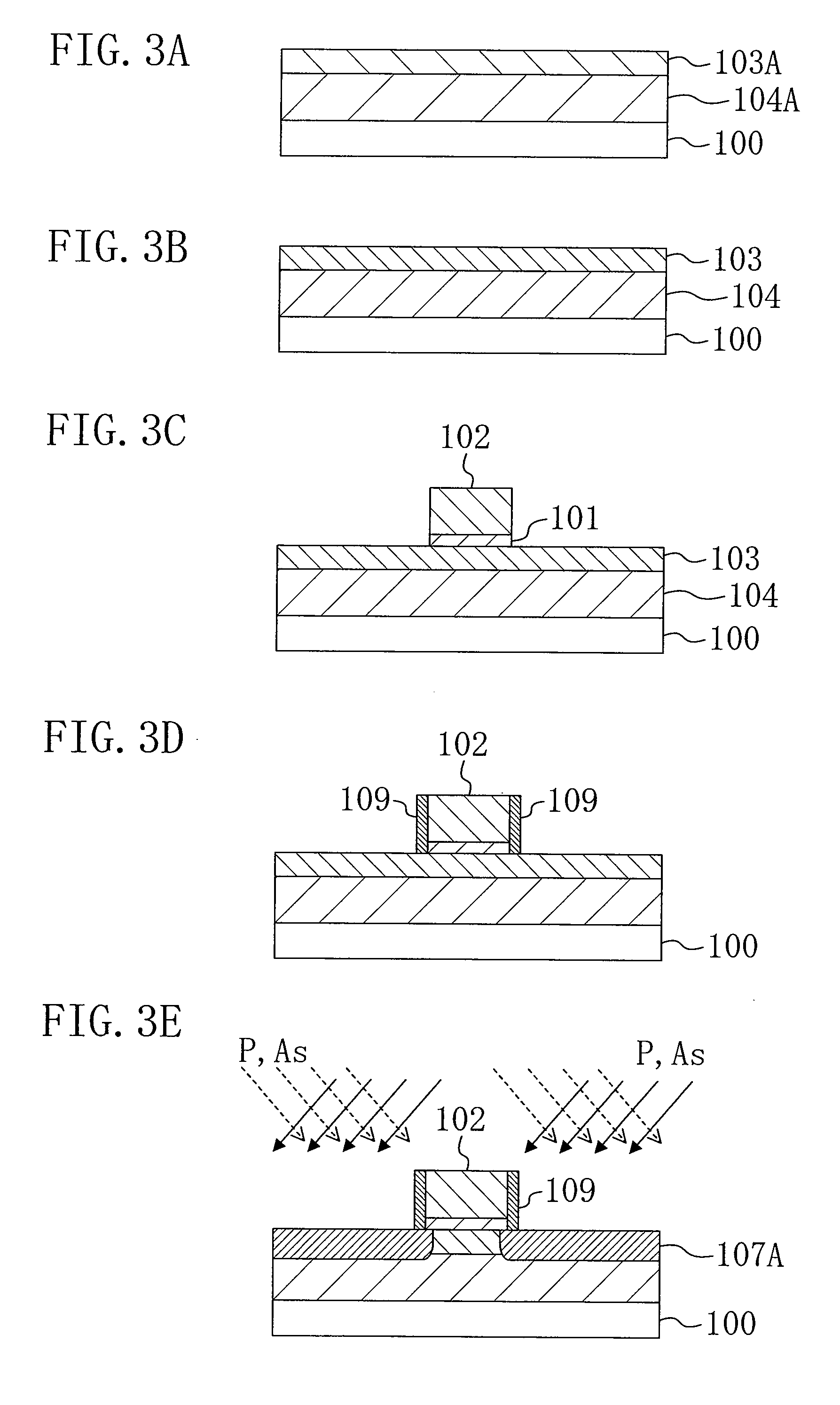
[0074]Hereinafter, a method for fabricating the semiconductor device of FIG. 1 will be described with reference to the drawings.

[0075]...

second embodiment

[0111]Hereinafter, a second illustrative embodiment will be described with reference to the drawings. A difference between the first and second embodiments will be described, referring to their fabrication methods.

[0112]FIGS. 9A to 9D and 10A to 10D are cross-sectional views showing a structure of a semiconductor device (MIS transistor) according to the second illustrative embodiment in the order in which major steps of a fabrication method thereof are performed.

[0113]Initially, as shown in FIG. 9A, as in the first embodiment, an N-type impurity (e.g., phosphorus (P) ions) is implanted by angled implantation into a semiconductor substrate 100 at an implantation energy of about 50 keV and an implantation dose of about 2×10¹³ / cm2 using offset spacers 109 and a gate electrode 102 as a mask. Next, an N-type impurity (e.g., arsenic (As) ions) is implanted by angled implantation at an implantation energy of about 80 keV and an implantation dose of about 1×10¹³ / cm2, thereby forming N-type ...

third embodiment

[0130]Hereinafter, a third illustrative embodiment will be described with reference to the drawings. A difference between the second and third embodiments will be described, referring to their fabrication methods.

[0131]FIGS. 11A to 11D and 12A to 12D are cross-sectional views showing a structure of a semiconductor device (MIS transistor) according to the third illustrative embodiment in the order in which major steps of a fabrication method thereof are performed.

[0132]Initially, as shown in FIG. 11A, as in the first embodiment, an N-type impurity (e.g., phosphorus (P) ions) is implanted by angled implantation into a semiconductor substrate 100 at an implantation energy of about 50 keV and an implantation dose of about 2×10¹³ / cm2 using offset spacers 109 and a gate electrode 102 as a mask. Next, an N-type impurity (e.g., arsenic (As) ions) is implanted by angled implantation at an implantation energy of about 80 keV and an implantation dose of about 1×10¹³ / cm2, thereby forming N-type...


PUM


Abstract

A semiconductor device includes a gate electrode provided on a semiconductor region with a gate insulating film being interposed therebetween, extension diffusion layers provided in regions on both sides of the gate electrode of the semiconductor region, a first-conductivity type first impurity being diffused in the extension diffusion layers, and source and drain diffusion layers provided in regions farther outside than the respective extension diffusion layers of the semiconductor region and having junction depths deeper than the respective extension diffusion layers. At least one of the extension diffusion layers on both sides of the gate electrode contains carbon.

Description

CROSS REFERENCE TO RELATED APPLICATIONS[0001]This application claims priority under 35 U.S.C. §119(a) on Patent Application No. 2008-121176 filed in Japan on May 7, 2008, the entire contents of which are hereby incorporated by reference.BACKGROUND OF THE INVENTION[0002]The present disclosure relates to a Metal Insulator Semiconductor (MIS) type semiconductor device that has a shallow junction depth and a low-resistant diffusion layer, and can be further miniaturized, and a method for fabricating the semiconductor device.[0003]As the scale of integration of semiconductor integrated circuits increases, there is a demand for further miniaturization of a MIS transistor. To achieve this, the MIS transistor needs to have an extension diffusion layer with a shallow junction depth and a low resistance.[0004]Hereinafter, a method for fabricating a conventional MIS transistor will be described with reference to the accompanying drawings.[0005]FIGS. 13A to 13D and 14A to 14D show cross-section...

Claims


Application Information

Patent Timeline
Patent Type & Authority Applications(United States)
IPC IPC(8): H01L29/78H01L21/336
CPCH01L21/26506H01L21/324H01L29/6659H01L29/66537H01L29/6653H01L21/2658H01L21/26566H01L21/26513
Inventor NODA, TAIJI
Owner TAIWAN SEMICON MFG CO LTD
Why Eureka
Try Eureka