Organic light-emitting device
- Summary
- Abstract
- Description
- Claims
- Application Information
AI Technical Summary
Benefits of technology
Problems solved by technology
Method used
Image

Examples
example 1
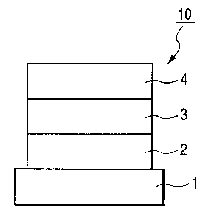
[0083]On a glass substrate, indium tin oxide (ITO) was formed into a film in a thickness of 120 nm as an anode 2 by a sputtering method. Next, the glass substrate having the ITO film formed thereon was ultrasonically cleaned sequentially with acetone and isopropyl alcohol (IPA), subsequently washed with boiled IPA, then dried, and further cleaned with UV / ozone. The glass substrate thus treated was used as a transparent conductive support substrate.
[0084]Next, as a hole-transporting layer, a film was formed in a thickness of 20 nm on the transparent conductive support substrate by spin coating of a solution of Compound 1 represented by the following formula in chloroform.
[0085]Further, other organic layers and an electrode layer serving as a cathode were successively formed by vacuum evaporation using resistive heating in a vacuum chamber at an inner pressure of 10−5 Pa to produce an organic light-emitting device. To be specific, first, as a light-emitting layer, a film was formed in...
example 2
[0088]A device was produced by following the same procedure as in Example 1 with the exception that Exemplified Compound No. A-11 shown below was used instead of Exemplified Compound No. A-2 as a guest for the light-emitting layer.
[0089]The device of this example was observed to emit green light with an emission luminance of 1,900 cd / m2 at an applied voltage of 6.0 V. Further, when a voltage was applied to the device in a nitrogen atmosphere at a current density of 30 mA / cm2 for 100 hours, the luminance was reduced from about 3,000 cd / m2 at an initial stage to about 2,900 cd / m2 after the elapse of the 100 hours, which meant that the luminance degradation was small. In addition, the device was observed to emit green light of good color purity with CIE chromaticity coordinates of x=0.35 and y=0.60.
example 3
[0090]A device was produced by following the same procedure as in Example 1 with the exception that Exemplified Compound No. B-20 shown below was used instead of Exemplified Compound No. A-2 as a guest for the light-emitting layer.
[0091]The device of this example was observed to emit green light with an emission luminance of 2,400 cd / m2 at an applied voltage of 6.0 V. Further, when a voltage was applied to the device in a nitrogen atmosphere at a current density of 30 mA / cm2 for 100 hours, the luminance was reduced from about 3,700 cd / m2 at an initial stage to about 3,550 cd / m2 after the elapse of the 100 hours, which meant that the luminance degradation was small. In addition, the device was observed to emit green light of good color purity with CIE chromaticity coordinates of x=0.30 and y=0.65.
PUM
| Property | Measurement | Unit |
|---|---|---|
| Efficiency | aaaaa | aaaaa |
Abstract
Description
Claims
Application Information