Laser-processed substrate for molecular diagnostics

a technology of molecular diagnostics and substrates, applied in the field of biomolecules, can solve the problems of insufficient specificity, inability to detect the exactness of the sample, and inability to accurately detect the sample, etc., and achieve the effect of facilitating the sers analysis of the sampl

Active Publication Date: 2009-11-12
EBSTEIN STEVEN M
View PDF42 Cites 35 Cited by
  • Summary
  • Abstract
  • Description
  • Claims
  • Application Information

AI Technical Summary

Benefits of technology

[0021]In one form of the invention, a means of introducing a cell or a solution or mixture (i.e., the analyte) to that nanostructured, metalized region is provided so that the analyte is either adsorb

Problems solved by technology

While current technology is quite useful, it is not as sensitive or as specific as is desired, and there is room for improvement in the speed and economics of the diagnostics.
The utility of many current genomic assays is limited by the need to replicate sample material using techniques like Polymerase Chain Reaction (PCR), which can add inaccuracies, take time to process, and may add cost through royalty payments.
One barrier to the use of Raman spectroscopy is the small cross-section for Raman scattering, a factor of ˜1014 less than the cross-section for fluorescence.
However, it is generally acknowledged that detailed knowledge and prediction of the s

Method used


Image

  • Laser-processed substrate for molecular diagnostics
  • Laser-processed substrate for molecular diagnostics
  • Laser-processed substrate for molecular diagnostics

Examples


Embodiment Construction

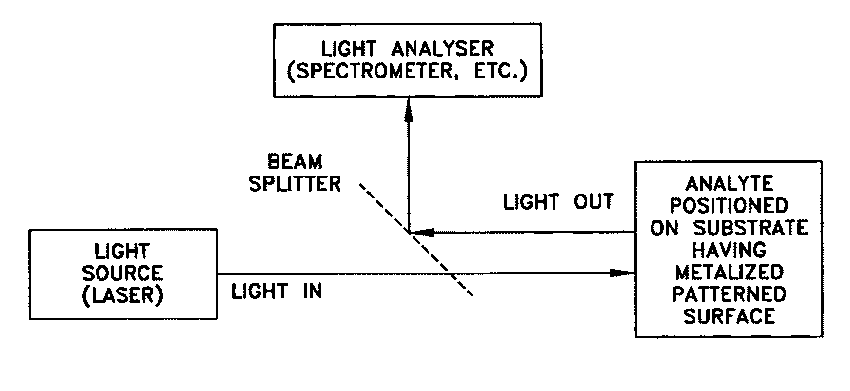
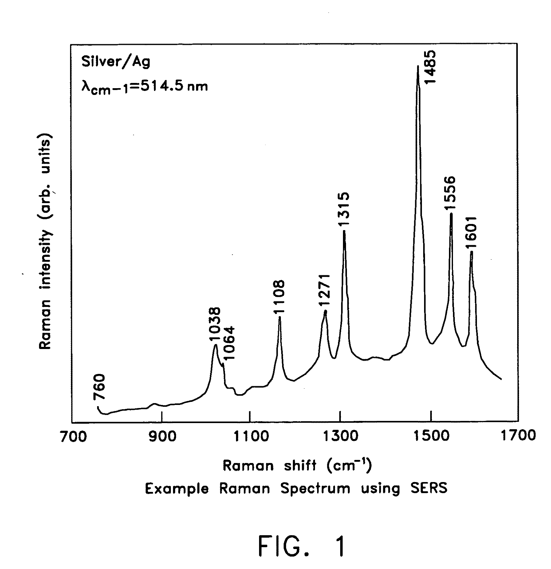
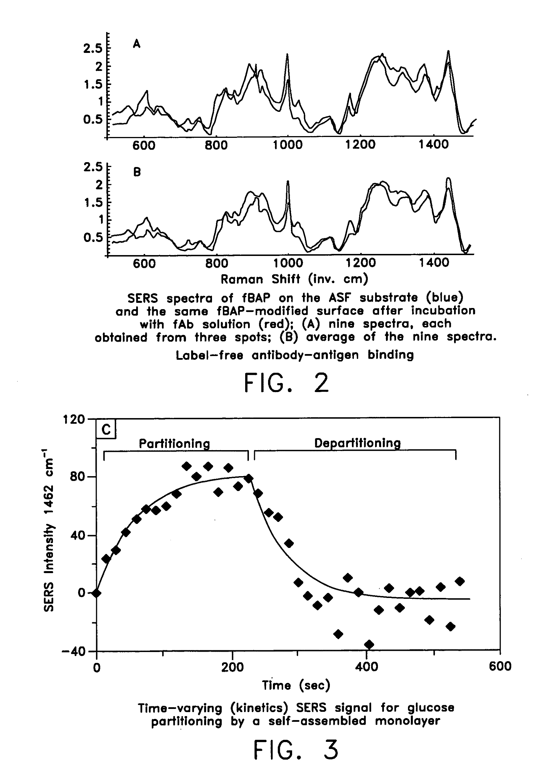
[0081]A novel substrate that meets all of the criteria discussed above for effecting surface enhancement of an analyte for SERS analyses is formed by a novel semiconductor or metal structure which includes nanopatterned surfaces fabricated by laser processing using femtosecond lasers. The femtosecond laser irradiation of the semiconductor or metal structure (e.g., silicon) in the appropriate environment can produce a variety of interesting nanostructures. These nanostructures are either produced in a metal substrate or the nanostructured surface is subsequently metalized so as to form the complete substrate which can provide the desired optical effect, e.g., for SERS applications.

[0082]One such structure is called black silicon, as micron-scale spikes formed on the surface of the silicon change the reflectivity of the silicon so its absorptance is significantly increased in the visible, and well into the infrared, spectrum.

[0083]Another structure has nanoscale bumps or spikes when t...


PUM


Abstract

Surface enhanced Raman Scattering (SERS) and related modalities offer greatly enhanced sensitivity and selectivity for detection of molecular species through the excitation of plasmon modes and their coupling to molecular vibrational modes. One of the chief obstacles to widespread application is the availability of suitable nanostructured materials that exhibit strong enhancement of Raman scattering, are inexpensive to fabricate, and are reproducible. I describe nanostructured surfaces for SERS and other photonic sensing that use semiconductor and metal surfaces fabricated using femtosecond laser processing. A noble metal film (e.g., silver or gold) is evaporated onto the resulting nanostructured surfaces for use as a substrate for SERS. These surfaces are inexpensive to produce and can have their statistical properties precisely tailored by varying the laser processing. Surfaces can be readily micropatterned and both stochastic and self-organized structures can be fabricated. This material has application to a variety of genomic, proteomic, and biosensing applications including label free applications including binding detection. Using this material, monolithic or arrayed substrates can be designed. Substrates for cell culture and microlabs incorporating microfluidics and electrochemical processing can be fabricated as well. Laser processing can be used to form channels in the substrate or a material sandwiched onto it in order to introduce reagents and drive chemical reactions. The substrate can be fabricated so application of an electric potential enables separation of materials by electrophoresis or electro-osmosis.

Description

REFERENCE TO PENDING PRIOR PATENT APPLICATIONS[0001]This patent application:[0002](i) is a continuation-in-part of pending prior U.S. patent application Ser. No. 11 / 452,729, filed Jun. 14, 2006 by Steven M. Ebstein for APPLICATIONS OF LASER-PROCESSED SUBSTRATE FOR MOLECULAR DIAGNOSTICS (Attorney's Docket No. EBSTEIN-1), which patent application in turn claims benefit of pending prior U.S. Provisional Patent Application Ser. No. 60 / 690,385, filed Jun. 14, 2005 by Steven M. Ebstein for APPLICATIONS OF LASER-PROCESSED SUBSTRATE FOR MOLECULAR DIAGNOSTICS (Attorney's Docket No. 2083 / 106; EBSTEIN-1 PROV); and[0003](ii) claims benefit of pending prior U.S. Provisional Patent Application Ser. No. 61 / 125,453, filed Apr. 25, 2008 by Steven M. Ebstein for APPLICATIONS OF LASER-PROCESSED SUBSTRATE FOR MOLECULAR DIAGNOSTICS (Attorney's Docket No. EBSTEIN-2 PROV).[0004]The three above-identified patent applications are hereby incorporated herein by reference.FIELD OF THE INVENTION[0005]The presen...

Claims


Application Information

Patent Timeline
IPC IPC(8): G01J3/44
CPCB01L3/5023B01L3/5027B01L3/502753B01L3/5088B01L2200/12G01N21/658B01L2400/0418B01L2400/0421B01L2400/086B82Y15/00B82Y30/00B01L2300/165
Inventor EBSTEIN, STEVEN M.
Owner EBSTEIN STEVEN M
Why Eureka
Try Eureka