Manufacturing method for micro-transformers

Inactive Publication Date: 2009-11-12
FUJI ELECTRIC CO LTD
View PDF4 Cites 18 Cited by
  • Summary
  • Abstract
  • Description
  • Claims
  • Application Information

AI Technical Summary

Benefits of technology

[0019]According to the fifth aspect of the invention, the secondary coil side can be adhered with reference to the pattern registering markers formed on the primary coil side. As a result, it is possible to eliminate the dislocation between the primary coil side and the secondary coil side.
[0020]A micro-transformer manufacturing method according to a sixth aspect of the invention is characterized in that, before the second insulating film is deposited, the size of the insulator material is worked to a size matching the pattern registering markers. According to the sixth aspect of the invention, in case the insulator material having the secondary coil formed is not transparent, the size of the

Problems solved by technology

However, the aforementioned manufacturing method of the related art is troubled by lowe

Method used


Image

  • Manufacturing method for micro-transformers
  • Manufacturing method for micro-transformers
  • Manufacturing method for micro-transformers

Examples


Example

Embodiment 1

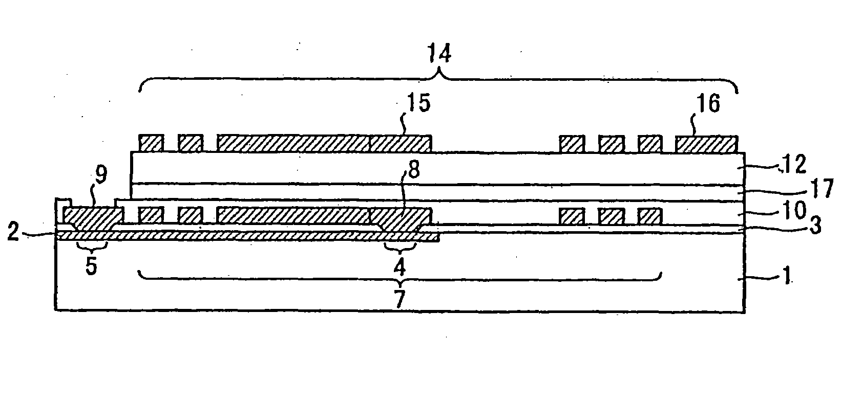
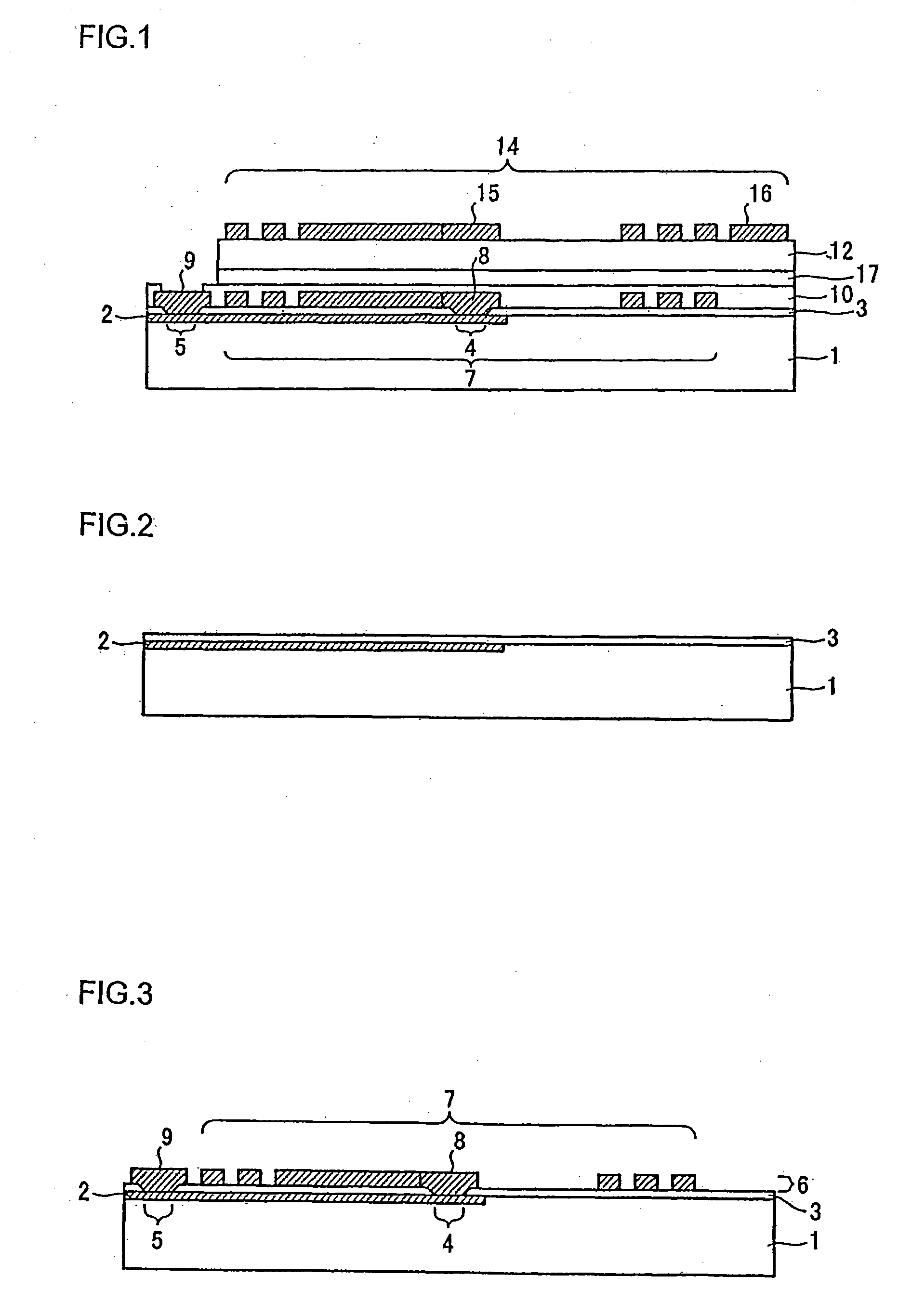
[0037]FIG. 1 is a sectional view showing the constitution of the micro-transformer manufactured by the manufacturing method according to Embodiment 1 of the invention. As shown in FIG. 1, the micro-transformer is equipped with a primary coil 7 and a secondary coil 14. The primary coil 7 and the secondary coil 14 are separated from each other by an insulating film 10, an adhesive tape 17 and an insulator material 12. Specifically, the insulating film 10 is made of an insulator such as an oxide, a nitride or polyimide. On the other hand, the insulator material 12 is specifically made of an insulator such as glass, quartz, sapphire, polyimide or ceramics, and is formed into a plate shape or a sheet shape. The adhesive tape 17 may be any type, if it is adhesive on its two faces and has a resistance to heat at subsequent bonding or the like. The adhesive tape 17 is specified by a DAF (Die Attach Film) tape or the like.

[0038]An impurity-diffused region 2 is selectively formed ...

Example

Embodiment 2

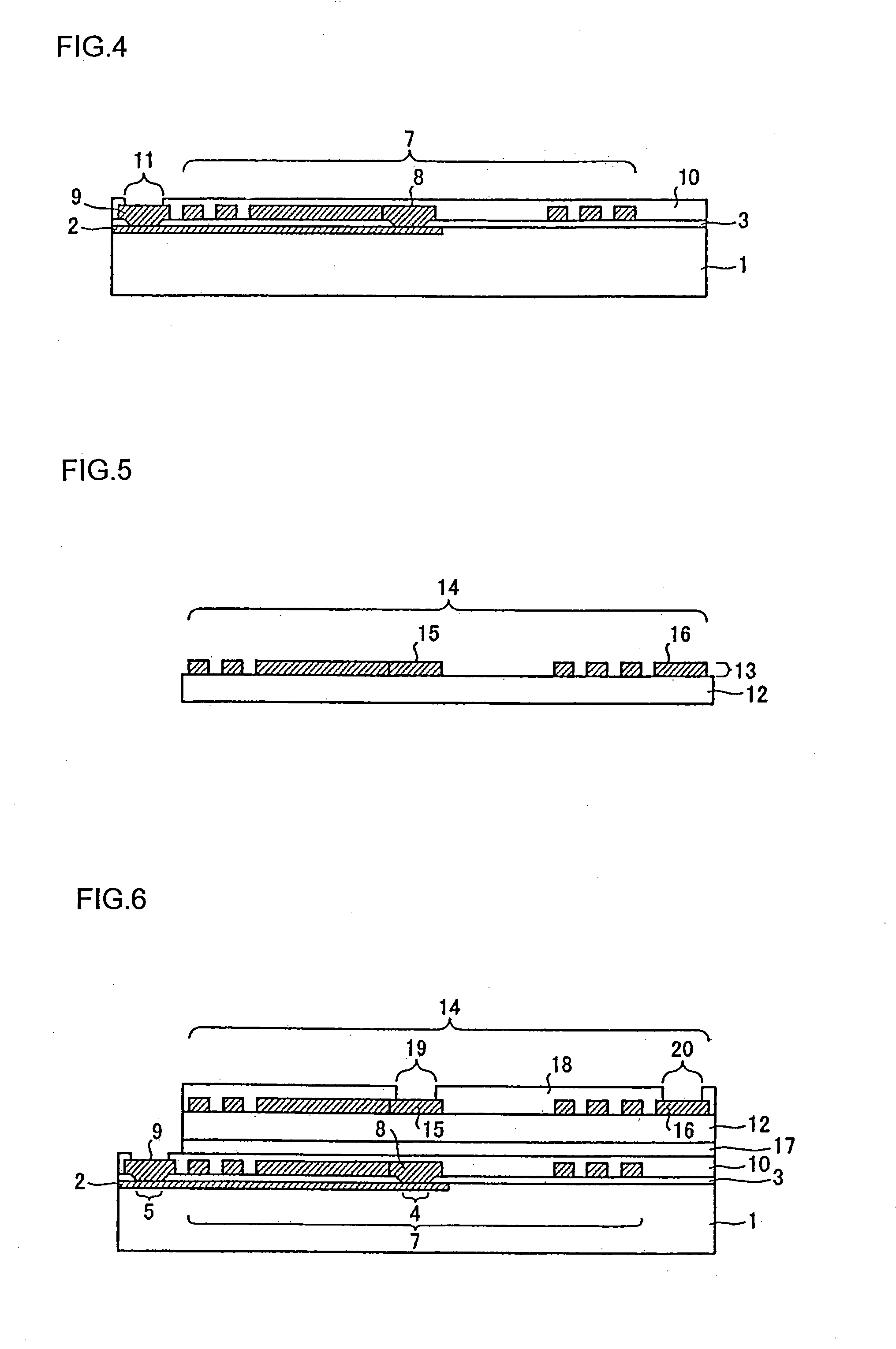
[0048]The constitution of the micro-transformer manufactured by the manufacturing method according to Embodiment 2 of the invention is omitted on its description, because it is similar to that of the micro-transformer manufactured by the manufacturing method of Embodiment 1. Embodiment 2 is different from Embodiment 1 in the thickness of the insulator material 12 to be prepared separately of the semiconductor substrate 1. In Embodiment 2, the manufacturing method of FIG. 2 to FIG. 4, as have been described in Embodiment 1, are performed first.

[0049]Next, the secondary coil 14 is formed on the surface of the insulator material 12, as shown in FIG. 5. An insulator material 12 is used that is thicker than the thickness necessary for the desired withstand voltage. Next, the face of that side of the insulator material 12 on which the secondary coil 14 is not formed is ground to work the insulator material 12 to a thickness necessary for the desired withstand voltage. Specific...

Example

Embodiment 3

[0051]FIG. 6 is a sectional view showing a constitution of the micro-transformer, which is manufactured by the manufacturing method according to Embodiment 3 of the invention. As shown in FIG. 6, the micro-transformer, as manufactured by the manufacturing method according to Embodiment 3, has an insulating film 18 deposited on the secondary coil 14 of the micro-transformer manufactured by the manufacturing method according to Embodiment 1 or 2. In this insulating film 18, an opening 19 is formed over the center pad 15 of the secondary coil 14. Moreover, an opening 20 is formed over the outer-end pad 16 of the secondary coil. In short, the center pad 15 and the outer-end pad 16 of the secondary coil 14 are exposed to the outside at the openings 19 and 20.

[0052]Embodiment 3 is different from Embodiment 1 or 2 in that the insulating film is formed over the secondary coil after this secondary coil is formed. In Embodiment 3, the same portions as those of Embodiment 1 or 2 ar...


PUM


Abstract

A micro-transformer manufacturing method is provided, which can improve throughput, prevent a crack from entering an insulating film between coils, and manufacture the micro-transformer without using a mask material having a high selection ratio. An insulating film is deposited on the whole face of a semiconductor substrate having an impurity-diffused region. This insulating film is partially removed to form a first opening and a second opening. A primary coil is formed such that a center pad contacts the impurity-diffused region through the first opening. A thin insulating film is deposited on the primary coil. An insulator material having a secondary coil formed thereon is adhered onto the insulating film on the primary coil by adhesive tape. The insulator material is sized to not cover both a pad, connected with the center pad of the primary coil through the impurity-diffused region, and an outer-end pad of the primary coil.

Description

BACKGROUND[0001]The invention relates to a method for manufacturing a micro-transformer to perform signal transmissions between electrically insulated electric circuits.[0002]In the related art, there are systems for performing signal transmissions between electrically insulated electric circuits so that a dangerous voltage may not pass when a high-voltage such as a surge is applied. One of those systems utilizes an inductive coupling by a transformer (as referred to in JP-A-11-196136 [corresponding to U.S. Pat. No. 6,389,063], for example).[0003]As the recent MEMS (Micro Electro Mechanical Systems) technique improves, the transformer becomes smaller. This makes it possible to integrate the transformer and an integrated circuit. In the following, this small-sized transformer will be called the micro-transformer, and the signal transmission system using the micro-transformer is called the micro-transformer system (as referred to, for example, in JP-B-2001-148277 and in “Key Technolog...

Claims


Application Information

Patent Timeline
IPC IPC(8): H01L21/283
CPCH01F27/2804H01F2027/2809H01L23/5227H01L23/60H01L2924/0002H01L23/645H01L2924/00
Inventor IWAYA, MASANOBUHIRUTA, REIKOUENO, KATSUNORIMOCHIZUKI, KUNIO
Owner FUJI ELECTRIC CO LTD
Why Eureka
Try Eureka