Method for producing group iii nitride semiconductor light emitting device, group iii nitride semiconductor light emitting device, and lamp

Active Publication Date: 2009-11-19
TOYODA GOSEI CO LTD
View PDF5 Cites 43 Cited by
  • Summary
  • Abstract
  • Description
  • Claims
  • Application Information

AI Technical Summary

Benefits of technology

[0050]According to the method of the present invention for producing a group III nitride semiconductor light emitting device, since it is a method in which a buffer layer is formed so as to have a composition of AlXGa1-XN (0≦X<1) by activating, with plasma, and thereby reacting at least a metallic Ga source and a gas containing a group V element, and an underlying layer that constitutes an n-type semiconductor layer is then formed on the buffer layer, the buffer layer can be formed as a layer with favorable orientation and an underlying layer w

Problems solved by technology

There is a large lattice mismatch between such a substrate made of different materials and the crystals of the group III nitride semiconductor epitaxially grown thereon.
In general, when there is a large lattice mismatch as in the above case, it will be difficult to directly grow crystals epitaxially on a substrate, and even when the crystals are grown, crystals with satisfactory crystallinity cannot be attained, which is a problem.
For this reason, distortions of crystals occur, as a result of which sufficient light emission cannot be achieved without the optimization of crystal structure, and the problems such as the decline in the productivity also arise.
However, since such a material is reactive with ammonia, Ga, hydrogen, or the like which is used in the MOCVD method as a source material at high temperatures, it has been difficult to grow the crystals, as i

Method used


Image

  • Method for producing group iii nitride semiconductor light emitting device, group iii nitride semiconductor light emitting device, and lamp
  • Method for producing group iii nitride semiconductor light emitting device, group iii nitride semiconductor light emitting device, and lamp
  • Method for producing group iii nitride semiconductor light emitting device, group iii nitride semiconductor light emitting device, and lamp

Examples


Example

Example 1

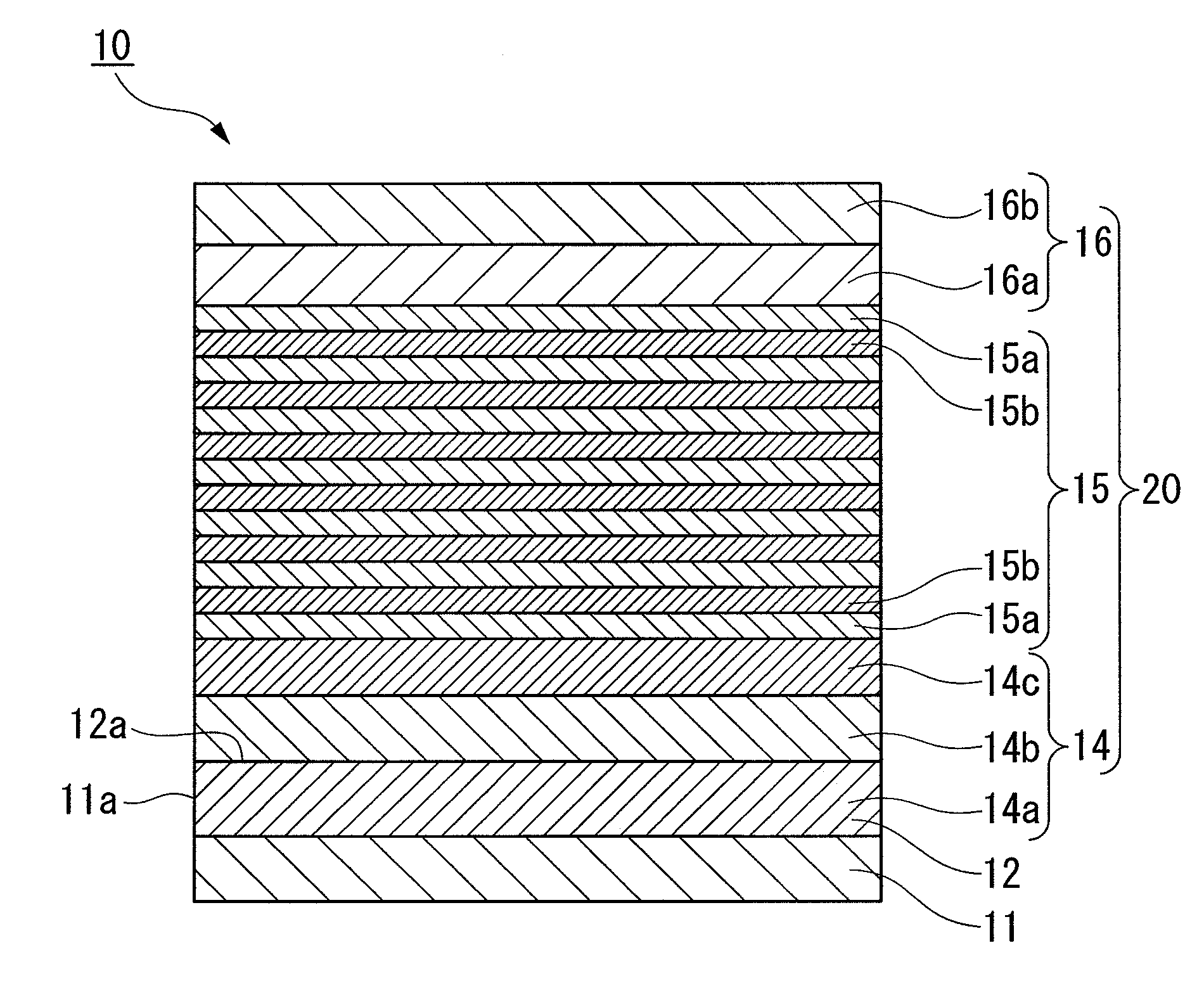
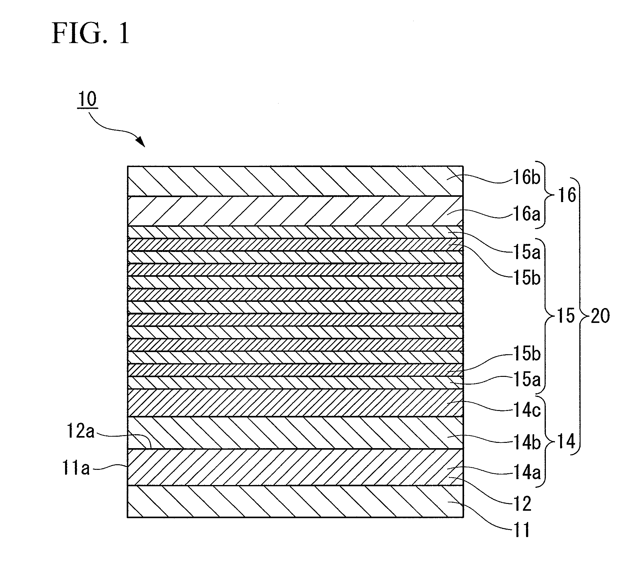
[0209]FIG. 1 shows a schematic cross sectional diagram of a laminated semiconductor formed of a group III nitride based compound semiconductor light emitting device produced in the present experimental example.

[0210]In the present example, a layer composed of GaN single crystal was formed as a buffer layer 12 on a c-plane of a substrate 11 composed of sapphire using an RF sputtering method, and a layer composed of GaN (group III nitride semiconductor) was then formed as an underlying layer 14a on top of the buffer layer 12 using an MOCVD method.

Formation of Buffer Layer

[0211]First, a substrate formed of a 2-inch diameter (0001) c-plane sapphire that had been polished to a mirror surface was placed inside a chamber. In this process, as a sputtering apparatus, as the sputtering apparatus 40 exemplified in FIG. 40, an apparatus having a high frequency power supply and a mechanism capable of moving the position of a magnet within a target was used. Note that a target formed of ...


PUM


Abstract

Provided is a method for producing a group III nitride semiconductor light emitting device capable of producing a group III nitride semiconductor light emitting device with excellent light emitting properties with excellent productivity; a group III nitride semiconductor light emitting device; and a lamp.
Provided is a method in which a buffer layer 12 composed of a group III nitride compound is laminated on a substrate 11 and then an n-type semiconductor layer 14 provided with an underlying layer 14a, a light emitting layer 15, and an p-type semiconductor layer 16 are sequentially laminated on the buffer layer 12, and is a method in which the buffer layer 12 is formed so as to have a composition of AlXGa1-XN (0≦X<1) by activating, with plasma, and thereby reacting at least a metallic Ga source and a gas containing a group V element, and the underlying layer 14 is formed on the buffer layer 12.

Description

BACKGROUND OF THE INVENTION[0001]1. Field of the Invention[0002]The present invention relates to a method for producing a group III nitride semiconductor light emitting device and a group III nitride semiconductor light emitting device which are suitably used for a light emitting diode (LED), a laser diode, an electronic device, or the like, and also relates to a lamp.[0003]2. Description of the Related Art[0004]A group III nitride semiconductor has a direct transition type band gap of energy that corresponds to a range from the visible light to an ultraviolet region and also has excellent light emission efficiency. For this reason, it is manufactured into a semiconductor light emitting device such as a light emitting diode (LED) and a laser diode (LD), and used in various applications. In addition, the group III nitride semiconductor also has a potential of achieving excellent characteristics when used in electronic devices, as compared to the case where a conventional group Ill-V ...

Claims


Application Information

Patent Timeline
IPC IPC(8): H01L33/00H01L21/20H01L33/06H01L33/12H01L33/22H01L33/32H01L33/42H01L33/62
CPCH01L21/0237H01L21/0242H01L2924/1305H01L2224/73265H01L2224/48091H01L2224/45144H01L2924/01079H01L21/0243H01L21/02458H01L21/02538H01L21/0254H01L21/02631H01L21/02658H01L33/007H01L33/12H01L2224/4823H01L2924/01004H01L2924/01012H01L2924/0102H01L2924/01025H01L2924/01057H01L2924/00H01L2924/00014
Inventor MIKI, HISAYUKIYOKOYAMA, YASUNORIOKABE, TAKEHIKOHANAWA, KENZO
Owner TOYODA GOSEI CO LTD
Why Eureka
Try Eureka