Nitride Semiconductor Light Emitting Element and Method for Producing Nitride Semiconductor Light Emitting Element

a light emitting element and semiconductor technology, applied in semiconductor/solid-state device manufacturing, semiconductor devices, electrical equipment, etc., can solve the problems of difficult to uniformly inject current into an active layer, difficult to produce single-crystalline bulk, and difficult to achieve light output efficiency. to increase

Active Publication Date: 2009-12-03
ROHM CO LTD
View PDF3 Cites 49 Cited by
  • Summary
  • Abstract
  • Description
  • Claims
  • Application Information

AI Technical Summary

Benefits of technology

[0011]However, although the above described method can reduce shear stress due to N2 gas during laser lift-off (LLO), thereby preventing cracks of the nitride semiconductor 23, a dry etching time is increased because the isolation trenches 24 for discharging N2 gas need to be formed until the isolation trenches 24 reach the sapphire substrate 21. Furthermore, a time period when a light emitting region side of the nitride semiconductor 23 is exposed to an etching gas (plasma) is increased and, therefore the light emitting region is damaged. This causes an increase in leakage current and ESD deterioration and luminance deterioration due to the increase in leakage current.
[0019]According to the present invention, n and p electrodes are disposed to be opposite to each other on a nitride semiconductor layer, and even for a nitride semiconductor light emitting element in which an isolation trench for chip separation or laser lift-off is formed by etching, the side face from a p electrode to a step position disposed on an n-type nitride semiconductor layer exceeding a light emitting region is covered with a protective insulating film, so the light emitting region and the like can be protected without exposing to etching gas for a long period of time.
[0020]In addition, when the second protective insulating film is formed on top of the outside of the first protective insulating film, if the refractive index of the second protective insulating film is made smaller than that of the first protective insulating film, a part of light emitted to the side face can be reflected by total reflection and taken out, whereby the light output efficiency can be increased.

Problems solved by technology

In nitride semiconductor manufacturing, bulk single crystal production is difficult, and thus GaN is grown on a different kind of substrate such as a sapphire substrate, or a SiC substrate by use of MOCVD (metal organic chemical vapor deposition).
However, the sapphire substrate is an insulating substrate and does not show conductivity, whereby electrodes cannot be disposed with the substrate intervening therebetween.
In the structure in which two electrodes of p and n types are disposed on the same face side as described above, however, currents tend to be concentrated on a mesa part close to the n electrode, whereby the ESD (electrostatic breakdown) voltage cannot be raised.
In addition, it is difficult to uniformly inject currents into an active layer and also difficult to cause the active layer to emit light uniformly.
Moreover, because sapphire has high hardness and a hexagonal crystal structure, the sapphire substrate needs to be separated into chips by scribing when sapphire is used for a substrate for growth, making manufacturing steps complicated and the yield bad.
However, even in this flip chip type, both the electrodes of p and n types are present on the same face side, whereby any of the above problems cannot be solved.
However, SiC of a conductive substrate usable for nitride gallium is costly at present and the amount of light absorption becomes large when an impurity is doped in a substrate to make the substrate conductive.
However, implementation of LLO decomposes a GaN buffer layer to generate N2 gas and thus applies shear stress to the GaN buffer layer and the nitride semiconductor, whereby the border part of a region irradiated with laser light frequently has cracks.

Method used


Image

  • Nitride Semiconductor Light Emitting Element and Method for Producing Nitride Semiconductor Light Emitting Element
  • Nitride Semiconductor Light Emitting Element and Method for Producing Nitride Semiconductor Light Emitting Element
  • Nitride Semiconductor Light Emitting Element and Method for Producing Nitride Semiconductor Light Emitting Element

Examples


Embodiment Construction

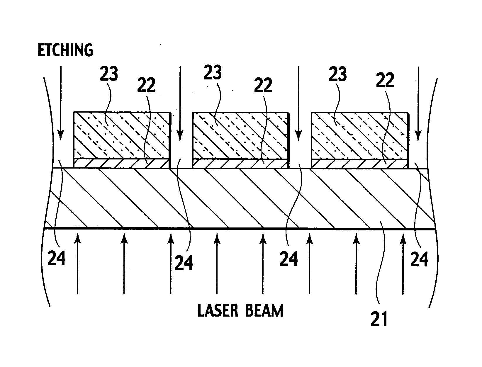
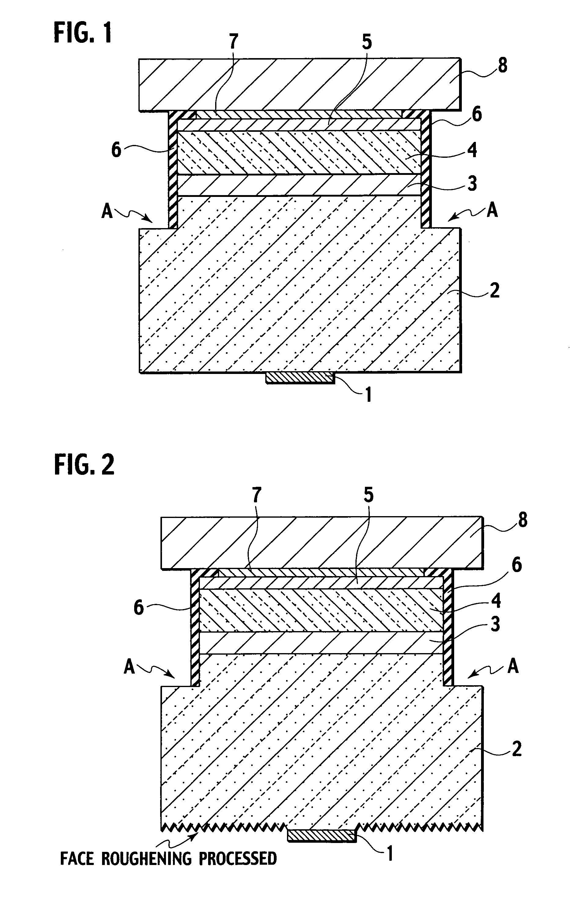
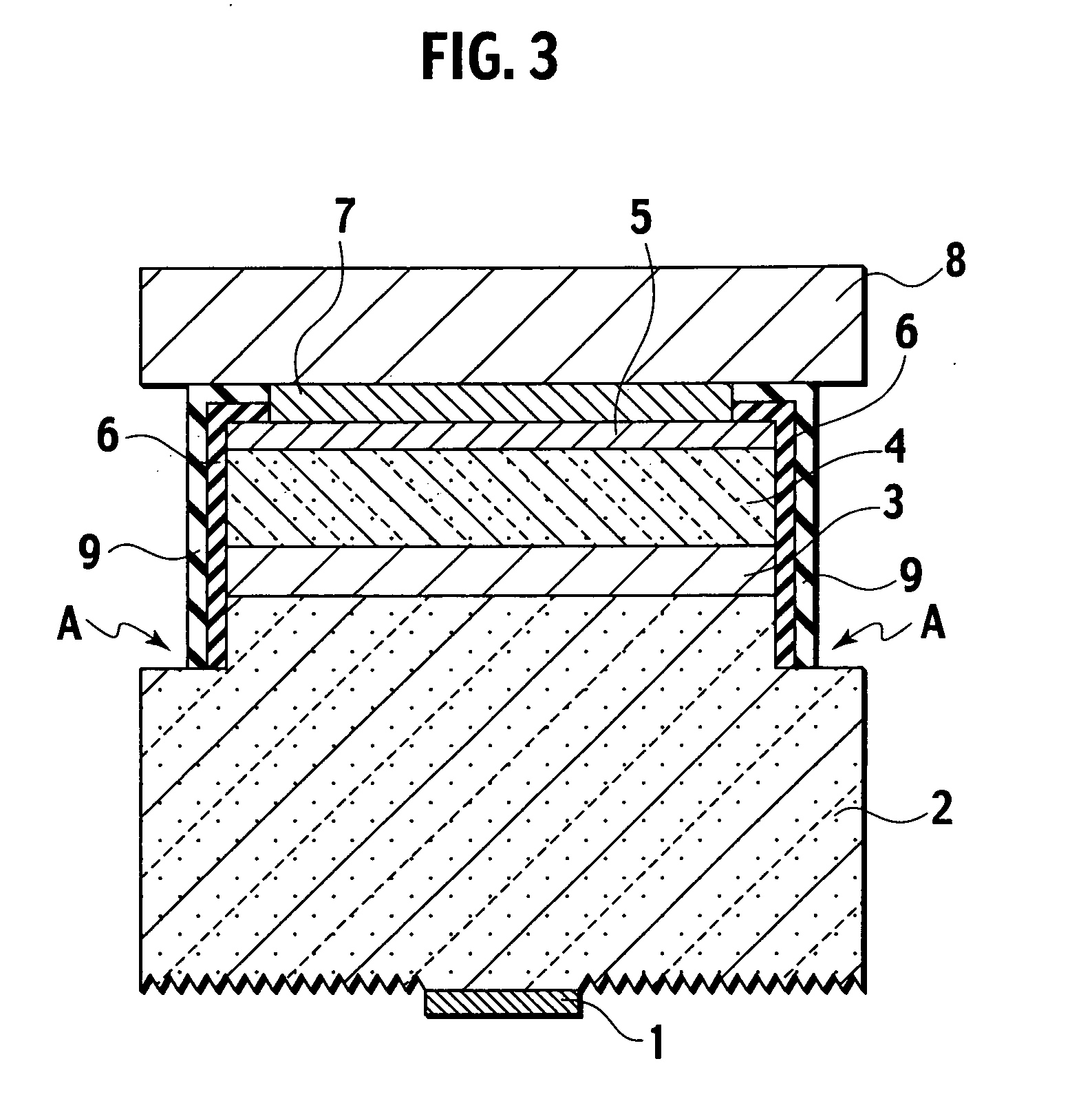
[0052]Hereinafter, one embodiment of the present invention will be described with reference to drawings. FIG. 1 shows a cross-sectional structure of a first nitride semiconductor light emitting element according to the present invention.

[0053]Nitride semiconductors also known as III-V group semiconductors include elements such as Al, Ga and In selected from the III group of the periodic table and an element N of the V group. The nitride semiconductor may be a binary alloy crystal such as gallium nitride (GaN), a tertiary alloy crystal such as aluminum gallium nitride (AlGaN) or indium gallium nitride (InGaN), or a quaternary alloy crystal such as aluminum gallium indium nitride (AlGaInN). These materials are deposited onto substrates to produce laminated semiconductor structures usable as light emitting elements used for opto-electronic devices. Nitride semiconductors have a wide band gap necessary for emission of visible light having a short wavelength in green-blue-violet-ultravio...


PUM


Abstract

Provided are a nitride semiconductor light emitting element which does not suffer a damage on a light emitting region and has a high luminance without deterioration, even though the nitride semiconductor light emitting element is one in which electrodes are disposed opposite to each other and an isolation trench for chip separation and laser lift-off is formed by etching; and a manufacturing method thereof. An n-type nitride semiconductor layer 2 has a step, formed in a position beyond an active layer 3 when viewed from a p side. Up to the position of this step A, a protective insulating film 6 covers a part of the n-type nitride semiconductor layer 2, the active layer 3, a p-type nitride semiconductor layer 4, the side of a p electrode 5 and a part of the top side of the p electrode 5. The use of a structure having a chip side face covered with the protective insulating film 6 prevents the active layer or the like from being exposed to an etching gas for a long time when an isolation trench for chip separation or laser lift-off is formed by etching.

Description

TECHNICAL FIELD[0001]The present invention relates to a nitride semiconductor light emitting element in which electrodes are disposed opposite to each other and a method for producing the nitride semiconductor light emitting element.BACKGROUND ART[0002]Nitride semiconductors are used in a blue LED, an LED and LD used for multi-color, and the like which are used as light sources of illumination and back light.[0003]In nitride semiconductor manufacturing, bulk single crystal production is difficult, and thus GaN is grown on a different kind of substrate such as a sapphire substrate, or a SiC substrate by use of MOCVD (metal organic chemical vapor deposition). Since exhibiting excellent stability in high-temperature ammonium atmospheres in epitaxial growth steps, a sapphire substrate is particularly used as a substrate for growth. However, the sapphire substrate is an insulating substrate and does not show conductivity, whereby electrodes cannot be disposed with the substrate interveni...

Claims


Application Information

Patent Timeline
Patent Type & Authority Applications(United States)
IPC IPC(8): H01L33/00H01L33/06H01L33/32H01L33/44
CPCH01L21/78H01L33/44H01L33/20H01L33/0095
Inventor NAKAHARA, KENYAMAGUCHI, ATSUSHI
Owner ROHM CO LTD
Why Eureka
Try Eureka