Wiring substrate, manufacturing method thereof, semiconductor device, and manufacturing method thereof

a manufacturing method and substrate technology, applied in weaving, synthetic resin layered products, printed element electric connection formation, etc., can solve the problems of resin-impregnated fibrous-body composite substrates that cannot function as sealing materials, air tightness cannot be maintained, and strength of resin-impregnated fibrous-body composite substrates can be decreased, so as to achieve the effect of maintaining mechanical strength, maintaining mechanical strength and air tightness

Inactive Publication Date: 2009-12-10
SEMICON ENERGY LAB CO LTD
View PDF19 Cites 20 Cited by
  • Summary
  • Abstract
  • Description
  • Claims
  • Application Information

AI Technical Summary

Benefits of technology

[0014]In a wiring substrate which uses a resin-impregnation fibrous-body composite material, even when a through wiring is provided, a strong wiring substrate capable of maintaining mechanical strength can be provided.

Problems solved by technology

However, formation of a through hole in a composite substrate, such as prepreg, in which a fibrous body is impregnated with a resin (hereinafter also referred to as a resin-impregnated fibrous-body composite substrate), damages a sheet-like fibrous body as a reinforcing material, whereby the strength of the resin-impregnated fibrous-body composite substrate is decreased.
In the case of using the resin-impregnated fibrous-body com

Method used


Image

  • Wiring substrate, manufacturing method thereof, semiconductor device, and manufacturing method thereof
  • Wiring substrate, manufacturing method thereof, semiconductor device, and manufacturing method thereof
  • Wiring substrate, manufacturing method thereof, semiconductor device, and manufacturing method thereof

Examples


embodiment 1

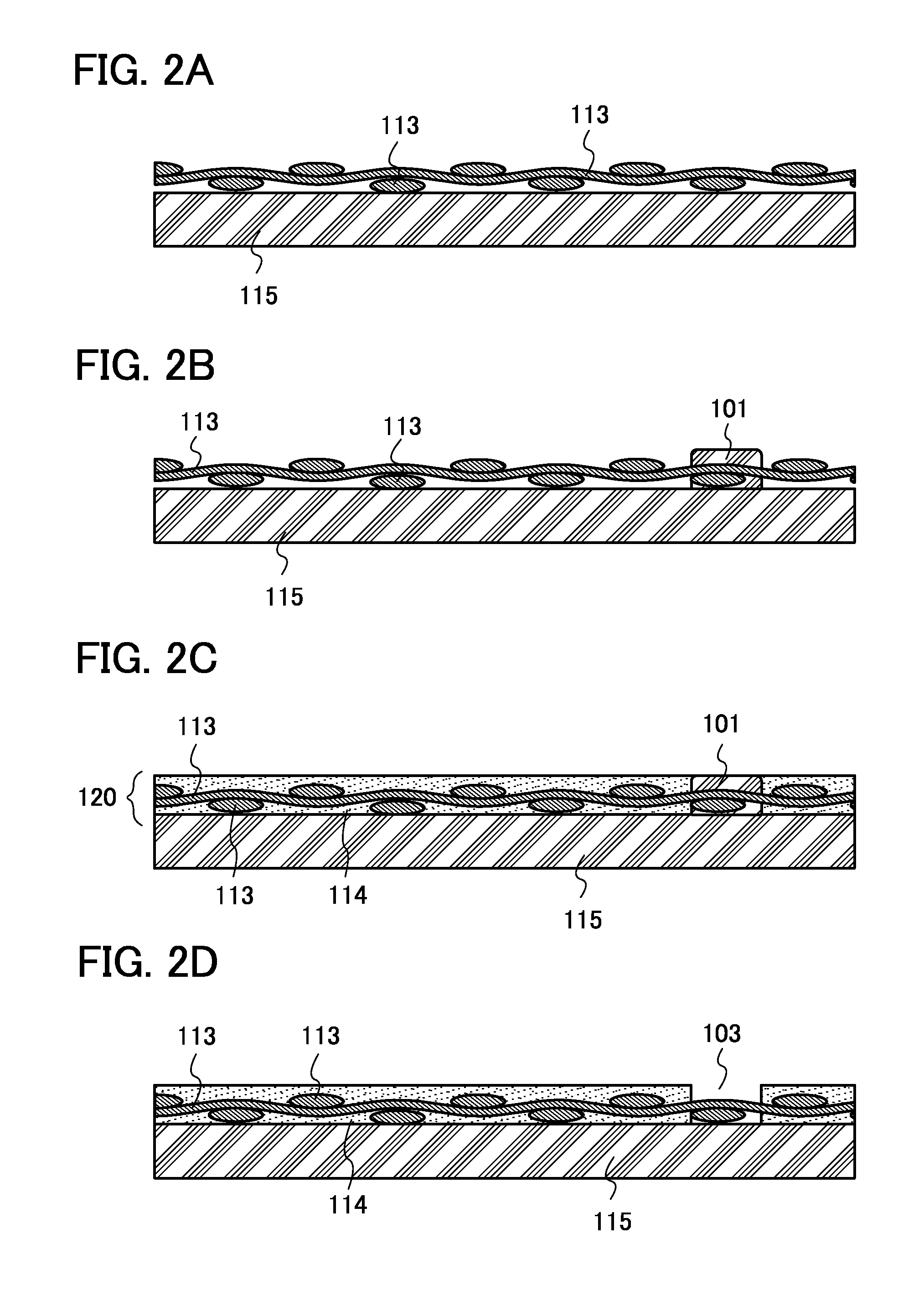
[0026]In Embodiment 1, the structure of a wiring substrate and manufacturing methods thereof will be described with reference to FIGS. 1A and 1B and FIGS. 2A to 2D.

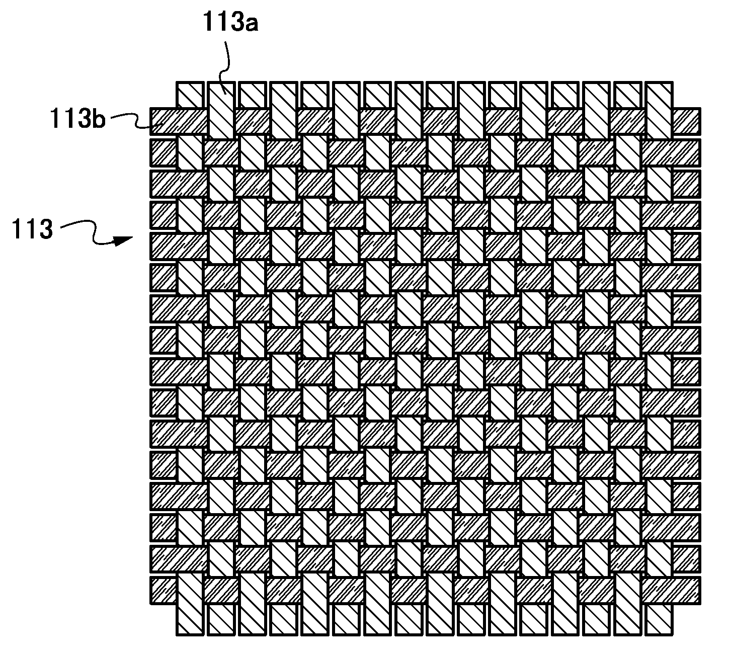
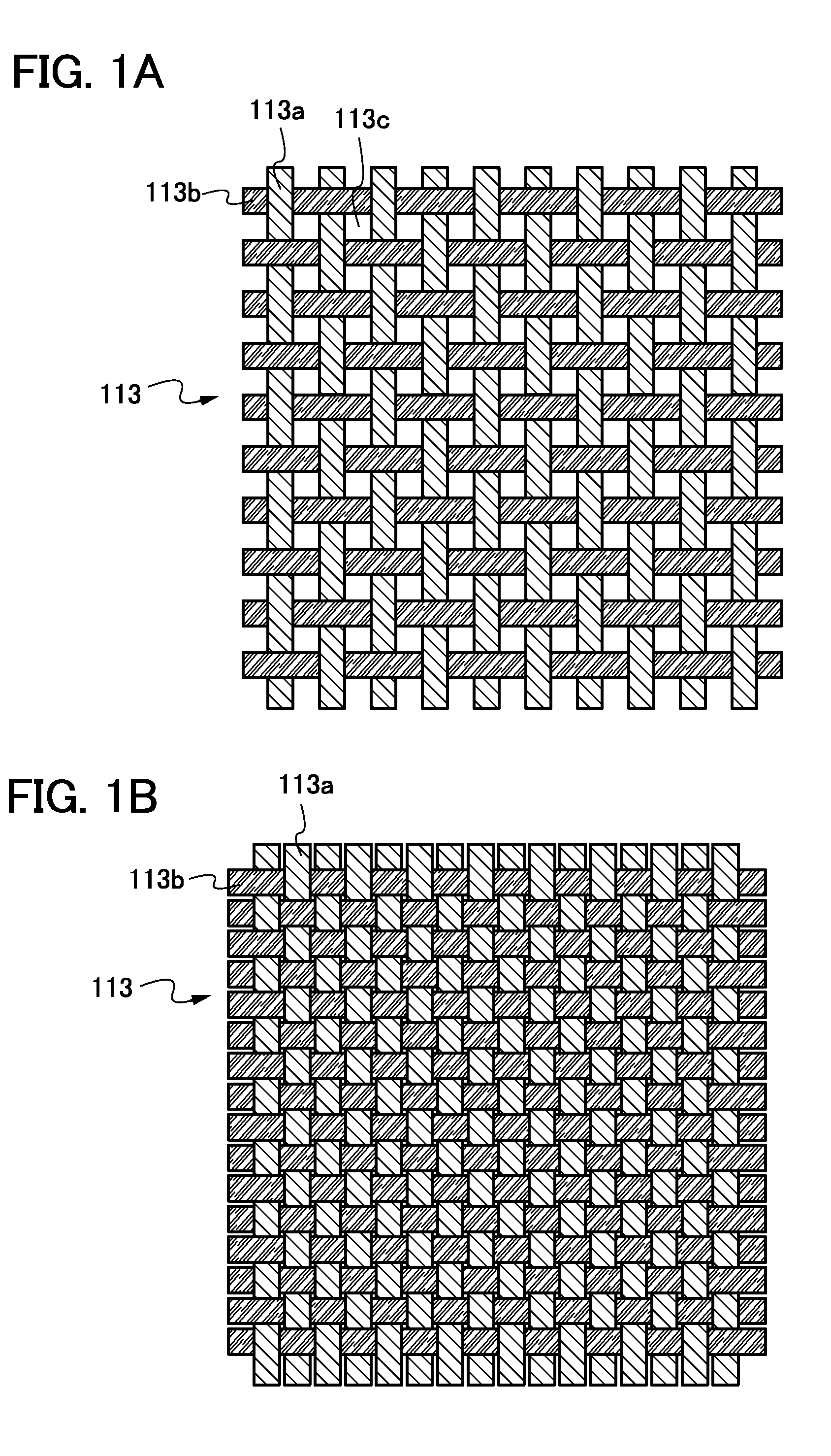
[0027]FIGS. 1A and 1B are each a top view of a sheet-like fibrous body 113 which is a fabric woven using yarn bundles for warp yarns and weft yarns.

[0028]The sheet-like fibrous body 113 is a woven fabric or a nonwoven fabric of an organic compound or an inorganic compound. Further, the sheet-like fibrous body 113 may be formed using a high-strength fiber.

[0029]The sheet-like fibrous body 113 may be formed using a woven fabric which is woven using bundles of fiber (single yarn) (hereinafter, referred to as yarn bundles) for warp yarns and weft yarns, or a nonwoven fabric obtained by stacking yarn bundles of plural kinds of fiber in a random manner or in one direction. In the case of a woven fabric, a plain-woven fabric, a twilled fabric, a satin-woven fabric, or the like can be appropriately used.

[0030]The yarn bundle may ...

embodiment 2

[0044]In Embodiment 2, a structure of a semiconductor device using a resin-impregnated fibrous-body composite substrate which is provided with a through wiring, and a manufacturing method thereof will be described with reference to FIGS. 3A to 3D, FIGS. 4A to 4E, FIGS. 5A to 5D, and FIGS. 7A and 7B.

[0045]FIGS. 3A to 3D are cross-sectional views of element layers according to this embodiment.

[0046]An element layer 51 includes a thin film transistor 52a, a thin film transistor 52b, an insulating film 65, an insulating film 66, and an insulating film 67 over an insulating layer 56. The thin film transistor 52a includes a semiconductor layer including impurity regions 53a which are a source region and a drain region and a channel formation region 63a, a gate insulating layer 54, and a gate electrode 55a. The thin film transistor 52b includes a semiconductor layer including impurity regions 53b which are a source region and a drain region and a channel formation region 63b, the gate insu...

example 1

[0110]The prepreg of Example 1 was manufactured in the following manner: a conductive resin was printed on a glass cloth, heating was performed, an insulating resin was printed, and then heating was performed.

[0111]As the conductive resin, silver paste including silver powder, 2-(2-butoxyethoxy)ethyl acetate, and an epoxy resin was used. As the insulating resin, an insulating resin including an epoxy resin and an amine curing agent was used.

[0112]FIG. 6A shows an optical micrograph of the thus-formed prepreg seen from the side on which the conductive resin is printed. FIG. 6B shows an optical micrograph seen from the rear side.

[0113]As shown in FIG. 6A, the conductive resin and the insulating resin were arranged without being mixed with each other.

[0114]In addition, it is seen from FIG. 6B that the conductive resin has gone through the glass cloth and is exposed on the rear surface.


PUM

PropertyMeasurementUnit
Electrical conductoraaaaaaaaaa

Abstract

A wiring substrate is provided, including an insulating resin layer which is provided on both surfaces of a sheet-like fibrous body and with which the sheet-like fibrous body is impregnated, and a through wiring provided in a region surrounded by the insulating resin layer. The through wiring is formed using a conductive material, the conductive material is exposed on both surfaces of the insulating resin layer, the sheet-like fibrous body is positioned in the conductive material, and the sheet-like fibrous body is impregnated with the conductive material. A manufacturing method of the wiring substrate is also provided.

Description

BACKGROUND OF THE INVENTION[0001]1. Field of the Invention[0002]The present invention relates to a wiring substrate which electrically or mechanically connects a semiconductor integrated circuit or a circuit substrate, and a semiconductor device using the wiring substrate.[0003]2. Description of the Related Art[0004]Prepreg in which a sheet-like fibrous body as a reinforcing material is impregnated with a thermosetting resin and the thermosetting resin is made in a semi-cured state has been used as a member of a circuit substrate and the like. For example, prepreg is known in which a conductor passes through an insulating layer and which is formed by opening a through hole in a predetermined position and filling the through hole with a conductive paste to become the conductor by hot pressing (see Patent Document 1). In this case, the through hole is opened in the prepreg by a laser, a drill, a punching machine, or the like.[0005]Further, prepreg used as a sealing material of a semic...

Claims


Application Information

Patent Timeline
IPC IPC(8): H01L23/12B32B5/02B05D5/12H01L21/58
CPCH01L21/6835H01L27/124H01L27/1266H01L29/78603H01L2221/6835H01L2224/29499H01L2924/09701H01L2924/14H01L2924/19041H01L2924/19043H01L2924/3025H05K1/0366H05K3/4069H05K3/4647H05K2201/029H05K2203/1147H01L2924/01067H01L2924/01068H01L2924/01079H01L23/3733H01L2924/12044Y10T442/2418H01L2924/00H05K1/11H05K3/40
Inventor CHIDA, AKIHIROAOKI, TOMOYUKI
Owner SEMICON ENERGY LAB CO LTD
Why Eureka
Try Eureka