Semiconductor device and manufacturing method of the same

a semiconductor and manufacturing method technology, applied in the direction of semiconductor devices, semiconductor/solid-state device details, resistor details, etc., can solve the problems of precision deterioration, the dependence of resistance value on upper and lower wiring pattern layout, and the influence of oxidation at the side surface portion unignorable, so as to prevent the increase of parasitic capacitance between metal wiring layers and the effect of reducing the resistance value due to the oxidation of metal resistor elements

Active Publication Date: 2009-12-10
HITACHI LTD
View PDF3 Cites 22 Cited by
  • Summary
  • Abstract
  • Description
  • Claims
  • Application Information

AI Technical Summary

Benefits of technology

[0014]According to the present invention, the increase of the resistance value due to the oxidation of the metal resistor element can be prevented, and at the same time, the increase of the parasitic capacitance between metal wiring layers can be prevented without complicating the fabrication process.

Problems solved by technology

However, since the ratio of the side-surface portion occupying the cross-sectional area of the resistor is inevitably increased when the line width of the resistor element is miniaturized, the influence of the oxidation at the side-surface portion becomes unignorable.
As described above, it has been revealed that, when a metal resistor element using a metal resistive element represented by TaN is fabricated in the LSI multilayer wiring structure, the problems of the dependence of the resistance value on the upper and lower wiring pattern layouts and the precision deterioration are caused by the miniaturization and the heat load.

Method used


Image

  • Semiconductor device and manufacturing method of the same
  • Semiconductor device and manufacturing method of the same
  • Semiconductor device and manufacturing method of the same

Examples


first embodiment

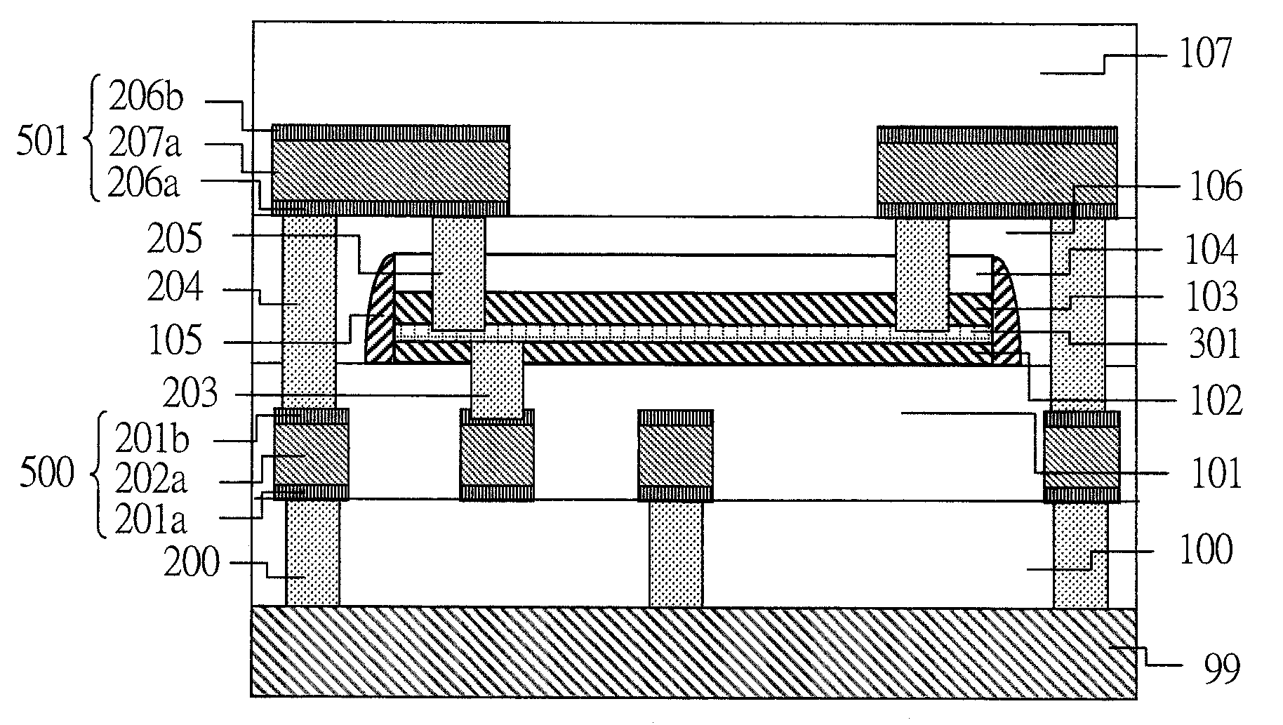
[0049]FIG. 1 is a schematic cross-sectional view of a semiconductor device according to the first embodiment of the present invention. Also, FIG. 7A to FIG. 7M are schematic cross-sectional views showing the manufacturing method of a semiconductor device according to the first embodiment of the present invention. The manufacturing method will be described below in due order.

[0050]FIG. 7A shows a multilayer wiring structure formed below a metal resistor element. First, after forming a first interlayer insulating film 100 of about 1000 nm made of a silicon nitride film or a silicon oxide film on a semiconductor substrate 99, first conductive contact hole plugs 200 each composed of a barrier film having a structure including a titanium film of about 30 nm and a titanium nitride film of about 100 nm deposited on the titanium film and tungsten are formed. Next, after a first aluminum alloy film 202a of about 500 nm and a first lower-layer barrier film 201a and a first upper-layer barrier...

second embodiment

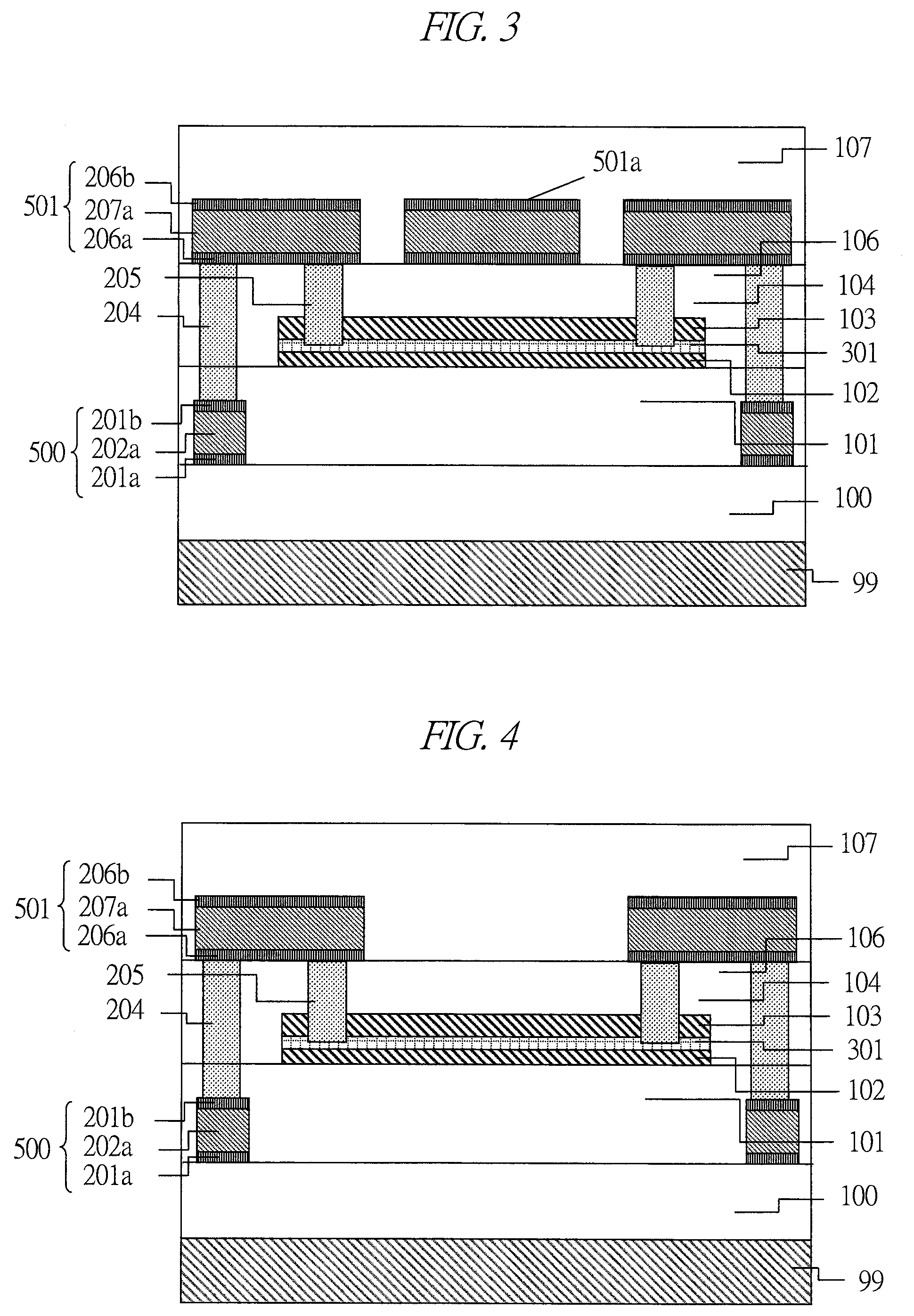
[0071]FIG. 9 is a schematic cross-sectional view showing a semiconductor device according to the second embodiment of the present invention. Also, FIG. 10A to FIG. 10L are schematic cross-sectional views showing the manufacturing method of the semiconductor device according to the second embodiment of the present invention. The manufacturing method will be described below in due order.

[0072]FIG. 10A shows a multilayer wiring structure formed below a metal resistor element. First, after forming a first interlayer insulating film 100 of about 1000 nm made of a silicon nitride film or a silicon oxide film on a semiconductor substrate 99, first conductive contact hole plugs 200 each composed of a barrier film having a structure including a titanium film of about 10 nm and a titanium nitride film of about 20 nm deposited on the titanium film and tungsten are formed. Next, a first damascene interlayer insulating film 101a made of a silicon oxide layer containing silicon oxide and fluorine...


PUM


Abstract

A semiconductor device according to the present invention includes: a lower-surface oxidation preventing insulating film formed on a lower surface of a metal resistor element; an upper-surface oxidation preventing insulating film formed on an upper surface of the metal resistor element; and a side-surface oxidation preventing insulating film formed only near a side surface of the metal resistor element by performing anisotropic etching after being deposited on a whole surface of a wafer in a process separated from the lower-surface oxidation preventing insulating film and the upper-surface oxidation preventing insulating film. According to the present invention, it is possible to prevent the increase of the resistance value due to the oxidation of the metal resistor element and also to prevent the increase of the parasitic capacitance between metal wiring layers without complicating the fabrication process.

Description

CROSS-REFERENCE TO RELATED APPLICATION[0001]The present application claims priority from Japanese Patent Application No. JP 2008-151225 filed on Jun. 10, 2008, the content of which is hereby incorporated by reference into this application.FIELD OF THE INVENTION[0002]The present invention relates to a semiconductor device in which a high-precision and high-performance resistor element is mounted and a manufacturing method of the semiconductor device.BACKGROUND OF THE INVENTION[0003]As for an RF analog LSI, to configure a circuit including high-performance capacitor element, resistor element and inductor element is an important factor. Particularly, the polysilicon resistor element has been conventionally used for the resistor element in a LSI, but the resistance value is fluctuated by the temperature increase due to the heat applied in the package mounting process and the self-heating caused by current flow, which poses a problem in configuring a high-precision analog circuit.[0004]J...

Claims


Application Information

Patent Timeline
Patent Type & Authority Applications(United States)
IPC IPC(8): H01C1/012
CPCH01L23/5228H01L27/0688H01L28/24H01L2924/0002H01L2924/00
Inventor FUJIWARA, TSUYOSHIIMAI, TOSHINORITAKEDA, KENICHISHIMAMOTO, HIROMI
Owner HITACHI LTD
Why Eureka
Try Eureka