Silicon single crystal manufacturing method, silicon single crystal, silicon wafer, apparatus for controlling manufacture of silicon single crystal, and program

a manufacturing method and single crystal technology, applied in the direction of non-metal conductors, oxide conductors, conductors, etc., can solve the problems of not necessarily providing a grown crystal having resistivity distribution, and the inability to obtain monocrystals having uniform resistivity distribution (i, polycrystals) to achieve the effect of improving operating efficiency

Active Publication Date: 2009-12-17
SUMCO TECHXIV
View PDF4 Cites 11 Cited by
  • Summary
  • Abstract
  • Description
  • Claims
  • Application Information

AI Technical Summary

Benefits of technology

[0018]Thus, a product-monocrystal having uniform resistivity can be provided even by recrystallizing in accordance with the FZ method a large-diameter ingot (raw material) having been pulled-up by CZ method, thereby suppressing the raw material cost irrespective of the large diameter of the product-monocrystal and reducing the manufacturing cost.
[0037]Thus, according to the aspect of the present invention, since the doping-gas flow rate can be suitably obtained in accordance with the resistivity distribution of the raw material having been pulled-up by the CZ method, the resistivity distribution of the product-monocrystal can be reliably made constant.
[0040]According to the aspect of the present invention, since the product-monocrystal can be manufactured while both of the theoretically-obtained doping-gas quantity and changes of the manufacturing conditions such as degradation of an induction-heating coil are taken into consideration at the time of recrystallizing by the FZ method, the resistivity distribution of the product-monocrystal in the length direction of the product can be more reliably made uniform.
[0051]According to the aspects of the present invention, by merely employing the above manufacturing-and-controlling apparatus in a facility for manufacturing silicon monocrystals by a typical FZ method or by merely installing the above program in a general-purpose manufacturing-and-controlling apparatus used for FZ method, the above-described effects and advantages can be obtained. In addition, since the doping-gas flow rate is automatically controlled, the raw material having been pulled-up by CZ method can be recrystallized by FZ method under an automatic control. With this arrangement, a great deal of improvement in operating efficiency can be expected.

Problems solved by technology

However, the technologies disclosed in Patent Documents 1 and 2 may not necessarily provide a grown crystal having resistivity distribution that is uniform in a longitudinal direction of the crystal.
Since the impurity distribution of the raw material is primarily ununiform, even by directly melting and recrystallizing the raw material by FZ method, a monocrystal having uniform resistivity distribution (i.e., a monocrystal that is comparable to a conventional product-monocrystal provided by using a gas doping method on a silicon polycrystal) may not be obtained.
Although the distribution of a monocrystal is improved by some degree by melting the raw material from a low-resistivity side of the raw material, such a monocrystal is not suitable for practical use.

Method used


Image

  • Silicon single crystal manufacturing method, silicon single crystal, silicon wafer, apparatus for controlling manufacture of silicon single crystal, and program
  • Silicon single crystal manufacturing method, silicon single crystal, silicon wafer, apparatus for controlling manufacture of silicon single crystal, and program
  • Silicon single crystal manufacturing method, silicon single crystal, silicon wafer, apparatus for controlling manufacture of silicon single crystal, and program

Examples


example 1

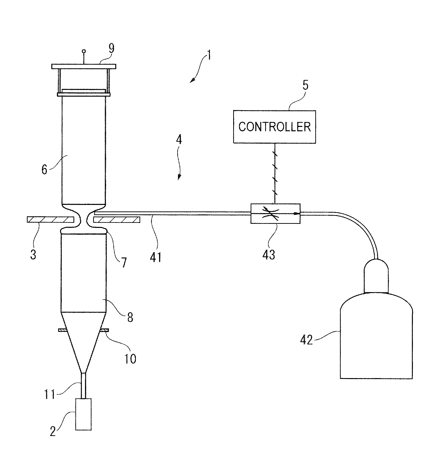
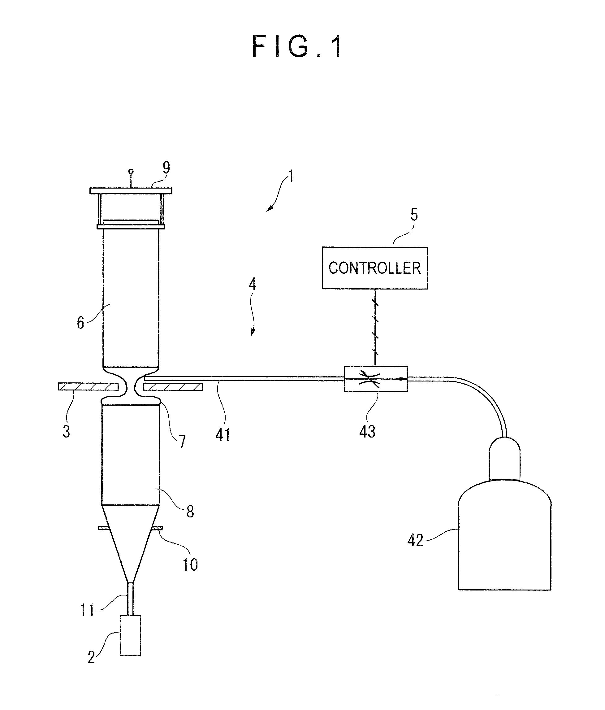
[0091]A product-monocrystal 8 having a diameter of 155 mm and a cylindrical length of 800 mm was manufactured by: tapering the high-resistivity side of the raw material 6; setting the gas flow rate based on the formula (13) with the target resistivity being 20 106·cm; flowing the doping gas into the furnace together with carrier gas (Ar) during the pulling-up at the gas flow rate set as a function of the length of the raw material 6; and zoning the raw material 6 at the crystal growth speed of 2.5 mm / min.

[0092]The gas flow rate, whose change is represented by the graph G1 of FIG. 1, was reduced as melting of the latter half of the raw material 6 went on. In FIG. 3, the tip end of the tapered portion of the raw material 6 corresponds to the material length of 0 while a position where gas flowing was started corresponds to a position where the entirety of the tapered portion had been melted.

example 2

[0093]A product-monocrystal 8 having a diameter of 155 mm and a cylindrical length of 800 mm was manufactured by: tapering the low-resistivity side of the same raw material 6 as that of the Example 1; setting the gas flow rate based on the formula (13) with the target resistivity being 20 Ω·cm; flowing the doping gas into the furnace together with carrier gas (Ar) during the pulling-up at the gas flow rate that was set as a function of the length of the raw material 6; and zoning the raw material 6 at the crystal growth speed of 2.5 mm / min.

[0094]The gas flow rate, whose change is represented by the graph G2 of FIG. 4, was increased as melting of the latter half of the raw material 6 went on. As in the Example 1, in FIG. 4, the tip end of the tapered portion of the raw material 6 corresponds to the material length of 0 while a position where gas flowing was started corresponds to a position where the entirety of the tapered portion had been melted.

example 3

[0095]Using the raw material 6 whose high-resistivity side was tapered as in the Example 1, a product-monocrystal 8 having a diameter of 155 mm and a cylindrical length of 800 mm was manufactured by setting the gas flow rate in the same manner as in the Example 1 and zoning the raw material 6 at the material growth speed of 2.5 mm / min.

[0096]As is represented by the graph of FIG. 3, the Example 3 differs from the Example 1 in that the gas was supplied in a quantity that was substantially twice as large as the gas quantity obtained by the formula (13) up to a position 50 mm away from the position where the entirety of the tapered portion had been melted. The gas quantity thereafter was the same as in the Example 1.

Comparative

[0097]In accordance with a typical FZ method, a product-monocrystal 8 having a diameter of 155 mm and a cylindrical length of 800 mm was manufactured from the raw material 6 whose low-resistivity side was tapered as in the Example 2 by zoning the raw material 6 at...


PUM

PropertyMeasurementUnit
diameteraaaaaaaaaa
diameteraaaaaaaaaa
resistivityaaaaaaaaaa

Abstract

A method of manufacturing a silicon monocrystal by FZ method, wherein a P-type or N-type silicon crystal having been pulled up by CZ method is used as a raw material. While impurities whose conductivity type is the same as that of the raw material are supplied by a gas doping method, the raw material is recrystallized by an induction-heating coil for obtaining a product-monocrystal.

Description

TECHNICAL FIELD[0001]The present invention relates to a method of manufacturing a silicon monocrystal, a silicon monocrystal, a silicon wafer, a silicon monocrystal manufacturing-and-controlling apparatus, and a program.BACKGROUND ART[0002]A silicon monocrystal has been widely used as a semiconductor material. According to a typical method of manufacturing a silicon monocrystal, a silicon-polycrystal material is recrystallized to be grown as monocrystal ingot(s). The obtained silicon monocrystal is sliced into wafers of a predetermined thickness.[0003]With respect to growing a silicon monocrystal, several technologies are under development so as to improve the quality thereof.[0004]In principle, a crystal grown by a floating zone (FZ) method can be made to have resistivity distribution that is uniform in a longitudinal direction of the grown crystal by using a gas doping method on a polycrystalline material having high resistivity.[0005]Meanwhile, in order to reduce manufacturing co...

Claims


Application Information

Patent Timeline
Patent Type & Authority Applications(United States)
IPC IPC(8): C30B13/00H01B1/08C30B15/30
CPCC30B13/12Y10T117/1008C30B29/06
Inventor TOGAWA, SHINJISATO, TOSHIYUKI
Owner SUMCO TECHXIV
Why Eureka
Try Eureka