Thin film transistor

a thin film transistor and transistor technology, applied in the field of thin film transistors, can solve the problems of low field-effect mobility and low on-current, low on-current, and inability to obtain sufficient switching characteristics, so as to achieve the effect of reducing the off increasing the on-current of the thin film transistor

Inactive Publication Date: 2009-12-31
SEMICON ENERGY LAB CO LTD
View PDF51 Cites 88 Cited by
  • Summary
  • Abstract
  • Description
  • Claims
  • Application Information

AI Technical Summary

Benefits of technology

[0038]As described above, as compared to a thin film transistor in which an amorphous semiconductor is included in a channel formation region, on-current of a thin film transistor can be increased. In addition, as compared to a thin film transistor in which a microcrystalline semiconductor is included in a channel formation region, off-current of a thin film transistor can be reduced.

Problems solved by technology

A thin film transistor in which a channel formation region is formed using an amorphous silicon layer has problems such as low field-effect mobility and low on-current.
On the other hand, a thin film transistor in which a channel formation region is formed using a microcrystalline silicon layer has a problem in that, whereas the field-effect mobility is higher than that of the thin film transistor in which a channel formation region is formed using an amorphous silicon layer, the off-current is high, and thus sufficient switching characteristics cannot be obtained.
However, the thin film transistor in which a channel formation region is formed using a polycrystalline silicon layer requires a crystallization step for a semiconductor layer and has a problem of higher manufacturing cost, as compared to the thin film transistor in which a channel formation region is formed using an amorphous silicon layer.
For example, a laser annealing technique involved in the process for forming a polycrystalline silicon layer has a problem in that large-screen liquid crystal panels cannot be produced efficiently because the laser beam irradiation area is small.

Method used


Image

  • Thin film transistor
  • Thin film transistor
  • Thin film transistor

Examples


embodiment 1

[0092]In Embodiment 1, an example of a mode of a thin film transistor will be described with reference to the drawings.

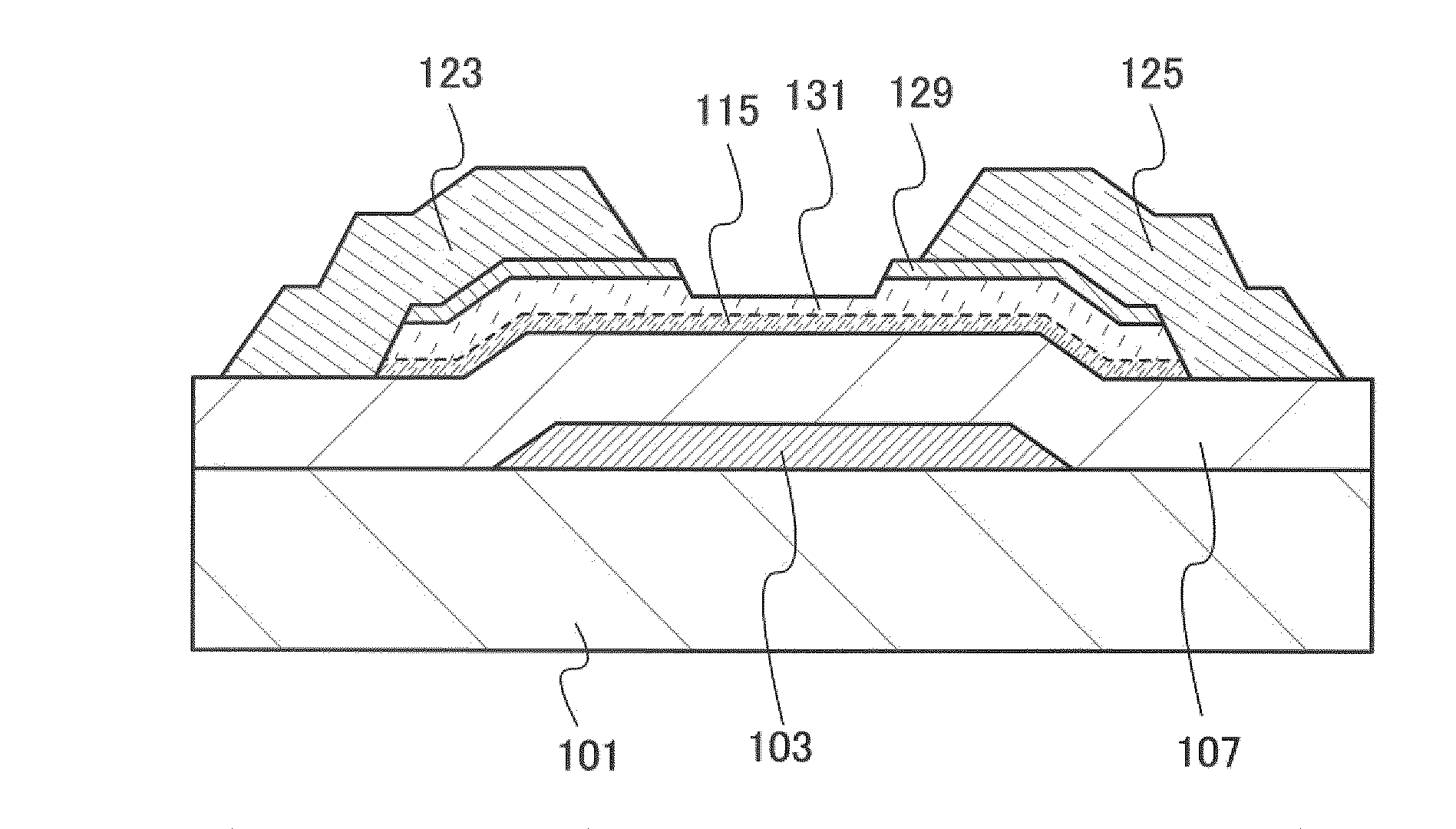
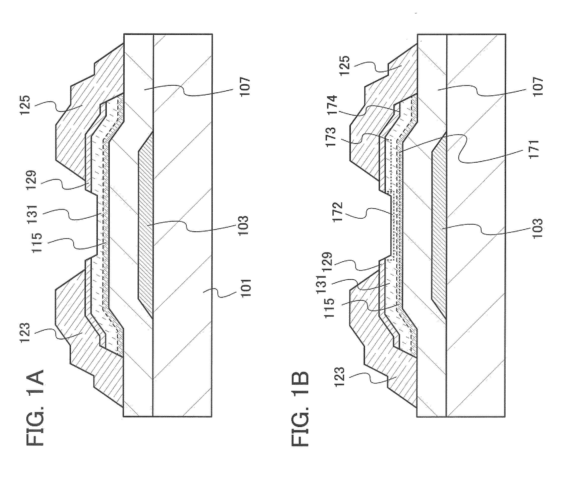
[0093]FIGS. 1A and 1B are cross-sectional views of a thin film transistor according to this embodiment. A thin film transistor illustrated in FIG. 1A includes a gate electrode layer 103 over a substrate 101; a gate insulating layer 107 covering the gate electrode layer 103; a semiconductor layer 115 which is provided over and in contact with the gate insulating layer 107 and serves as a channel formation region; a buffer layer 131 over the semiconductor layer 115; and source and drain regions 129 which are provided over and in contact with part of the buffer layer 131. In addition, the thin film transistor includes a wiring layer 123 and a wiring layer 125 which are provided over and in contact with the source and drain regions 129. The wiring layer 123 and the wiring layer 125 form a source electrode and a drain electrode. Further, each layer is patterned into a de...

embodiment 2

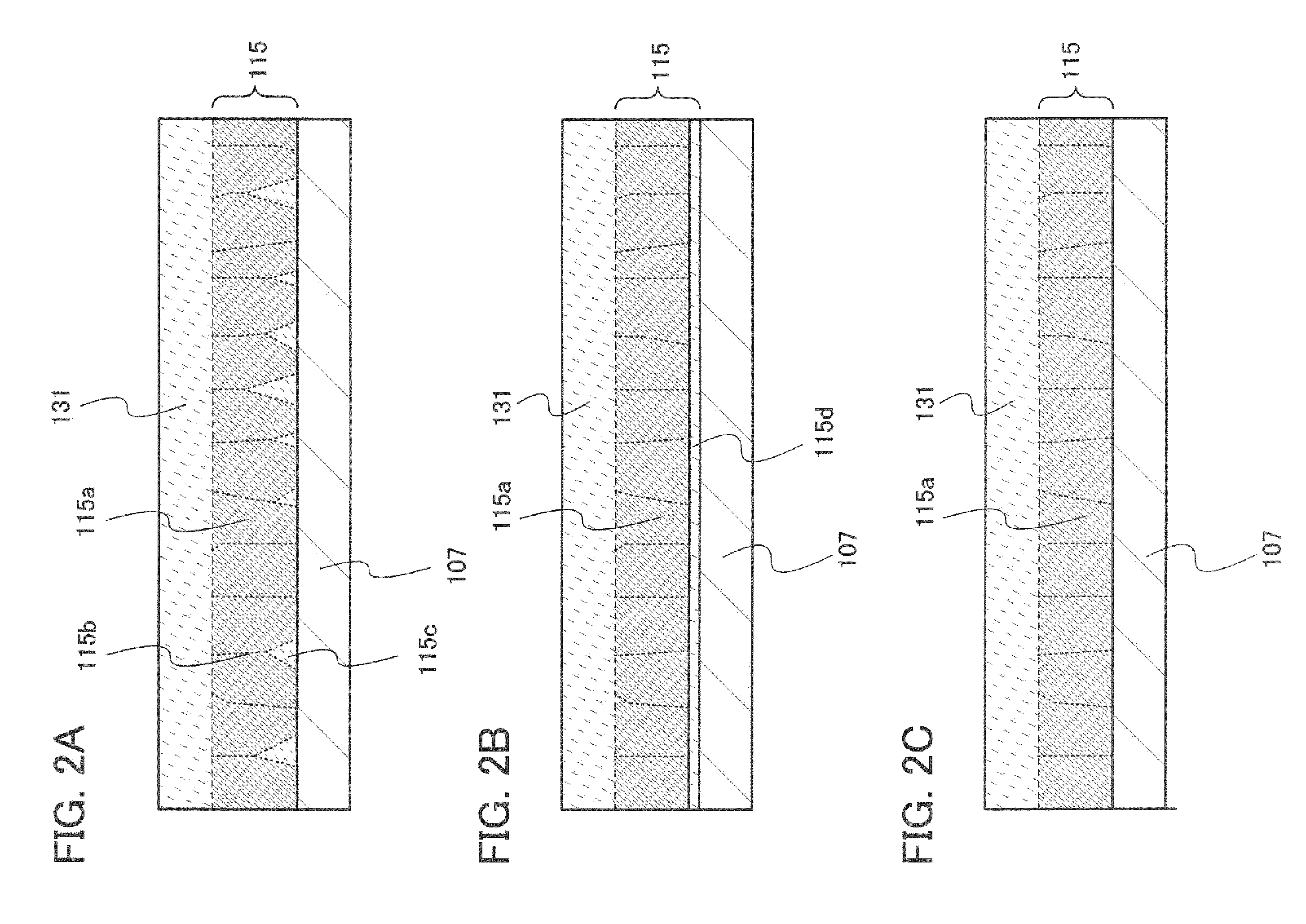
[0183]In Embodiment 2, modes which can be used for the semiconductor layer 115 in the thin film transistor described in Embodiment 1 will be described with reference to FIG. 9 and FIGS. 10A and 10B.

[0184]In a thin film transistor described in this embodiment, dispersed microcrystalline semiconductor particles or a net-like microcrystalline semiconductor 118 are / is formed over the gate insulating layer 107 (FIG. 9).

[0185]Dispersed microcrystalline semiconductor particles 118a illustrated in FIG. 10A or a net-like microcrystalline semiconductor 118b illustrated in FIG. 10B can be formed using silicon, silicon germanium (SixGe1-x, 0.5118a has a circular shape as illustrated in FIG. 10A and a cross section thereof has a hemispherical shape as illustrated in FIG. 9. When the diameter of the dispersed microcrystalline semiconductor particles viewed from above is set at 1 to 30 nm and the density thereof is set at less than 1×10¹³ / cm3, preferably less than 1×10¹⁰ / cm3, the dispersed microcr...

embodiment 3

[0191]In Embodiment 3, a thin film transistor in which the semiconductor layer 115 of Embodiment 1 is formed using a semiconductor layer including crystal regions in an amorphous structure, that is, a thin film transistor in which the semiconductor layer including crystal regions in an amorphous structure is formed between a gate insulating layer and source and drain regions will be described with reference to FIG. 11.

[0192]FIG. 11 is a cross-sectional view of a thin film transistor according to this embodiment. A thin film transistor illustrated in FIG. 11 includes a gate electrode layer 103 over a substrate 101; a gate insulating layer 107 covering the gate electrode layer 103; a semiconductor layer 132 which is provided over and in contact with the gate insulating layer 107; and source and drain regions 129 which are in contact with part of the semiconductor layer 132. In addition, the thin film transistor includes a wiring layer 123 and a wiring layer 125 which are provided over...


PUM


Abstract

A thin film transistor includes, as a buffer layer, a semiconductor layer which contains nitrogen and includes crystal regions in an amorphous structure between a gate insulating layer and source and drain regions, at least on the source and drain regions side. As compared to a thin film transistor in which an amorphous semiconductor is included in a channel formation region, on-current of a thin film transistor can be increased. In addition, as compared to a thin film transistor in which a microcrystalline semiconductor is included in a channel formation region, off-current of a thin film transistor can be reduced.

Description

TECHNICAL FIELD[0001]The present invention relates to a thin film transistor and a method for manufacturing the thin film transistor, and a semiconductor device and a display device using the thin film transistor.BACKGROUND ART [0002]As a kind of field-effect transistor, a thin film transistor in which a channel formation region is formed in a semiconductor layer formed over a substrate having an insulating surface is known. Techniques in which amorphous silicon, microcrystalline silicon, or polycrystalline silicon is used for the semiconductor layer used in the thin film transistor have been disclosed (Patent Documents 1 to 5). A typical application of a thin film transistor is a liquid crystal television device, and the thin film transistor has been put to the practical use as a switching transistor for each pixel included in a display screen.REFERENCE [Patent Document][0003][Patent Document 1] Japanese Published Patent Application No. 2001-053283[0004][Patent Document 2] Japanese...

Claims


Application Information

Patent Timeline
Patent Type & Authority Applications(United States)
IPC IPC(8): H01L29/04
CPCH01L27/1214H01L29/04H01L27/1288H01L29/78696H01L29/66765H01L29/78678
Inventor ISA, TOSHIYUKIJINBO, YASUHIROTEZUKA, SACHIAKIDAIRIKI, KOJIMIYAIRI, HIDEKAZUYAMAZAKI, SHUNPEIHIROHASHI, TAKUYA
Owner SEMICON ENERGY LAB CO LTD
Why Eureka
Try Eureka