Chamfering Apparatus For Silicon Wafer, Method For Producing Silicon Wafer, And Etched Silicon Wafer

a technology of chamfering apparatus and silicon wafer, which is applied in the direction of manufacturing tools, transportation and packaging, and cellulosic plastic layered products, etc. it can solve the problems of liquid tending to leak from the chamfering portion of the wafer, cracks in the wafer, and wafer cracks, etc., to achieve the effect of suppressing variations in cross-sectional shape dimensions

Active Publication Date: 2009-12-31
SHIN-ETSU HANDOTAI CO LTD
View PDF7 Cites 30 Cited by
  • Summary
  • Abstract
  • Description
  • Claims
  • Application Information

AI Technical Summary

Benefits of technology

[0021]The present invention has been made in view of the problem described above, and an object thereof is to provide a chamfering apparatus for a silicon wafer, production method and an etched silicon wafer that can suppress variations in the cross-sectional shape dimensions of a chamfered portion after an etching process, in order to achieve the precision of the cross-sectional shape of a wafer chamfered portion, the precision required by the customer.
[0023]With the above-described silicon wafer chamfering apparatus, unlike a conventional apparatus which uniformly chamfers a outer edge of a silicon wafer, the relative position of the outer edge of the silicon wafer and the chamfering grindstone at the time of chamfering is controlled and changed depending on the circumferential position of the silicon wafer, making it possible to perform chamfering in such a way as to change the chamfered shape of the outer edge of the silicon wafer depending on the circumferential position of the silicon wafer. Therefore, a silicon wafer whose chamfered shape is intentionally changed depending on the circumferential position can be obtained, and it is possible to obtain, after etching, an etched silicon wafer in which variations in the cross-sectional shape dimensions of the chamfered portion are suppressed to a minimum.
[0029]As described above, by obtaining the amount of change in shape caused by etching depending on the circumferential position of the silicon wafer by conducting a test in advance, it is possible to obtain the amount of change in shape caused by etching depending on the circumferential position of the silicon wafer accurately. This makes it possible to obtain a silicon wafer whose chamfered portion has cross-sectional shape dimensions with higher precision.
[0031]As described above, by performing the etching step by using a sodium hydroxide solution and / or a potassium hydroxide solution, it is possible to perform etching while relatively suppressing a change in shape of the principal surface of the silicon wafer caused by etching processing, and thereby obtain a wafer with a high degree of flatness.

Problems solved by technology

In exposure using this technology, if a wafer chamfered portion varies in shape, the liquid tends to leak from the wafer chamfered portion when the outermost edge of the wafer is scanned.
In this case, larger thermal shock than in the past acts on the silicon wafer, causing a crack in the wafer.
At the same time, as the conveyance-related speed is improved, a wafer crack may occur due to a contact between a wafer chamfered portion and a conveying portion or a wafer carrier.
This is because acid etching may reduce the flatness of the principal surface.
Therefore, with the above-described conventional production method, it was impossible to meet the recent demands to reduce variations in the cross-sectional shape dimensions of the chamfered portion to extremely small variations, for example, to +25 μm or less for the 32 nm node.

Method used


Image

  • Chamfering Apparatus For Silicon Wafer, Method For Producing Silicon Wafer, And Etched Silicon Wafer
  • Chamfering Apparatus For Silicon Wafer, Method For Producing Silicon Wafer, And Etched Silicon Wafer
  • Chamfering Apparatus For Silicon Wafer, Method For Producing Silicon Wafer, And Etched Silicon Wafer

Examples


Embodiment Construction

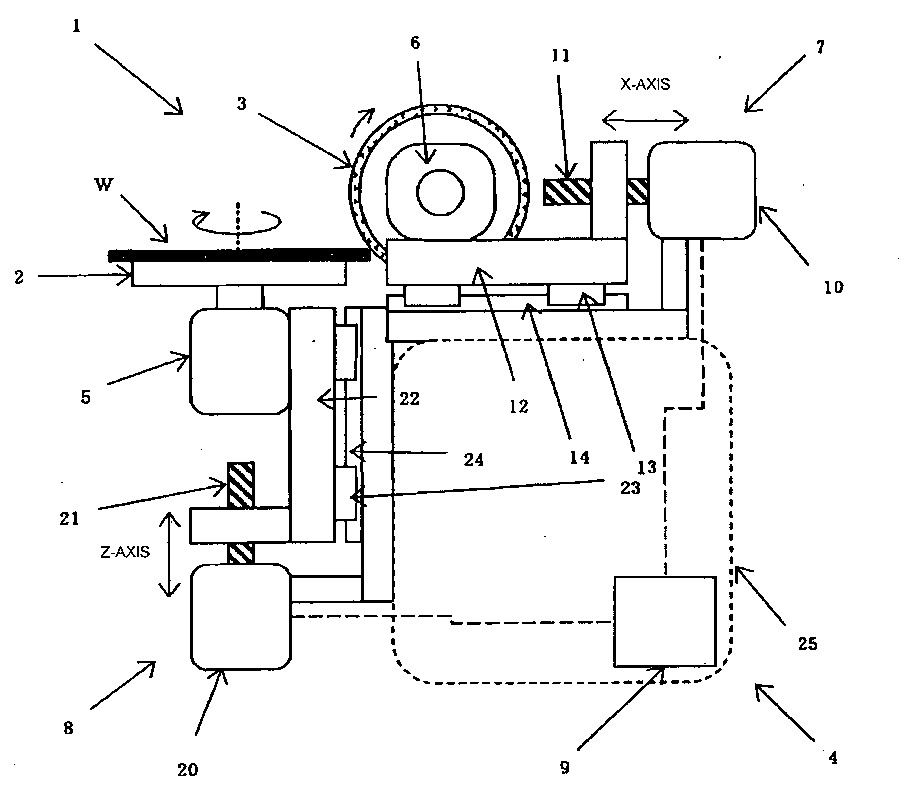
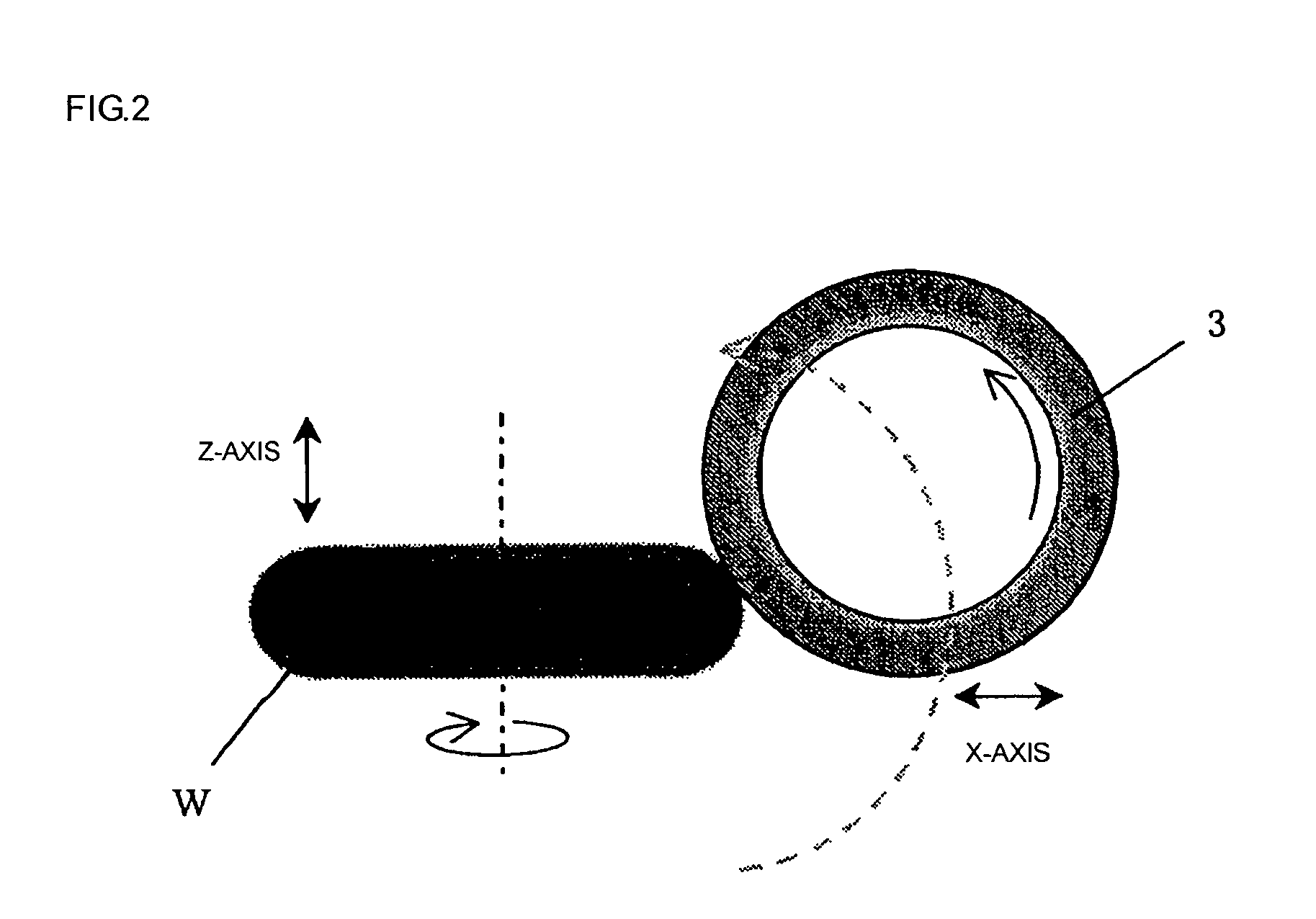
[0054]Hereinafter, an embodiment of the invention is explained; the invention, however, is not limited thereto.

[0055]In a conventional silicon wafer production method, it is common practice to chamfer the outer edge of a silicon wafer in each of circumferential positions into a uniform shape in a chamfering process, and then perform an etching process by alkali etching that is highly capable of maintaining the shape of the principal surface.

[0056]However, even when the uniform chamfered shape is obtained by the chamfering process, in the etching process that follows, due to crystal orientation-dependent etching anisotropy of an alkalie solution, the cross-sectional shape dimensions of the chamfered portion vary. As a result, although the conventional method maintains the flatness of the principal surface, it cannot meet the demands for high-precision cross-sectional shape dimensions of the chamfered portion.

[0057]Therefore, the inventor conducted a study on the chamfering process an...


PUM

PropertyMeasurementUnit
diameteraaaaaaaaaa
distanceaaaaaaaaaa
distanceaaaaaaaaaa

Abstract

The invention is directed to a chamfering apparatus for a silicon wafer to chamfer outer edge of a silicon wafer by using a chamfering grindstone, the chamfering apparatus including at least: a holder holding and rotating a silicon wafer; a chamfering grindstone chamfering the outer edge of the silicon wafer held by the holder; and a control apparatus for controlling a chamfered shape by controlling a relative position of the outer edge of the silicon wafer and the chamfering grindstone by numerical control, wherein the control apparatus controls and changes the relative position of the outer edge of the silicon wafer and the chamfering grindstone at the time of chamfering depending on the circumferential position of the silicon wafer held by the holder, a production method, and an etched silicon wafer. This provides a silicon wafer chamfering apparatus, production method and an etched silicon wafer that can suppress variations in the cross-sectional shape dimensions of a chamfered portion after an etching process.

Description

TECHNICAL FIELD[0001]The present invention relates to chamfering apparatuses for a silicon wafer which chamfer the outer edge of a silicon wafer, methods for producing a silicon wafer, and etched silicon wafers and, in particular, to a chamfering apparatus, a production method, and an etched silicon wafer relating to the cross-sectional shape of a chamfered portion of a silicon wafer.BACKGROUND ART[0002]In an advanced device adopting a large diameter silicon wafer typified by a silicon wafer having a diameter of 300 mm, for example, a stepper adopting a technology (immersion exposure technology) for enhancing the resolution by sandwiching liquid (normally, pure water) between an objective lens and a silicon wafer is gradually being adopted. In exposure using this technology, if a wafer chamfered portion varies in shape, the liquid tends to leak from the wafer chamfered portion when the outermost edge of the wafer is scanned. Thus, many device makers are required to conduct a review,...

Claims


Application Information

Patent Timeline
Patent Type & Authority Applications(United States)
IPC IPC(8): B32B5/00B24B49/00B24B9/08B44C1/22B24B9/00H01L21/304H01L21/306
CPCB24B9/065Y10T428/24777H01L21/02021B24B9/00H01L21/02H01L21/304
Inventor KATO, TADAHIRO
Owner SHIN-ETSU HANDOTAI CO LTD
Why Eureka
Try Eureka