Removal method of surface damage of single crystal diamond

Inactive Publication Date: 2010-01-07
NAT INST OF ADVANCED IND SCI & TECH
View PDF3 Cites 3 Cited by
  • Summary
  • Abstract
  • Description
  • Claims
  • Application Information

AI Technical Summary

Benefits of technology

[0059]According to the process of the invention, it is possible to substantially completely remove defects present in the surface layer of a single-crystal diamond.
[0060]In particular, when the substrate to be processed is a single-crystal diamond synthesized by a CVD method, in which the linear dislocation pattern that indicates the propagation of dislocations runs in parallel with the substrate surface,

Problems solved by technology

This is because, during the device fabrication process, a conductivity-controlled single-crystal film is, in general, grown by epitaxial growth on a substrate; any defects present inside the substrate or on the substrate surface are continued in an epitaxial growth film grown thereon, causing degradation of the crystal quality of these films.
The obtained substrates (plates), however, contain a certain amount of surface damage introduced by cutting and polishing, but no method for reducing or removing this damage has been disclosed.
Even with these methods, however, it is usually difficult to remove processing damage introduced bey

Method used


Image

  • Removal method of surface damage of single crystal diamond
  • Removal method of surface damage of single crystal diamond

Examples


example 1

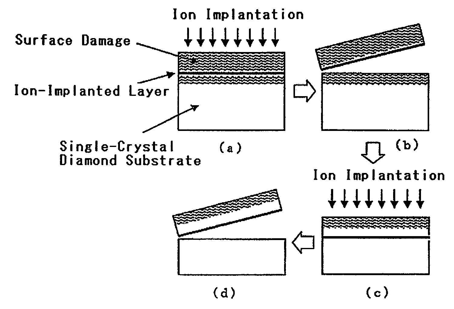
[0064]An Ib single-crystal diamond (100) substrate, synthesized by a high-temperature high-pressure synthesis method, and mechanically polished to a size of 9.3×9.5×1.05 mm3, was used as a substrate to be processed, and the removal of surface damage was performed according to the following process.

[0065]First, carbon ions were implanted into the single-crystal diamond substrate at an energy level of 3 MeV and a dose of 2×10¹⁶ ions / cm2, using a 1.5 MV tandem accelerator. The calculated value of the depth of implanted ions was about 1.6 μm. This irradiation caused the color of the diamond substrate to change from pale yellow to black, thus confirming the formation of a non-diamond layer.

[0066]Next, the single-crystal diamond substrate was heat-treated using a commercial microwave plasma CVD apparatus, causing the graphitization of the non-diamond layer to proceed. The heat treatment was performed for 25 minutes at a substrate temperature of 1,130° C., a pressure of 24 kPa, and a hydro...

example 2

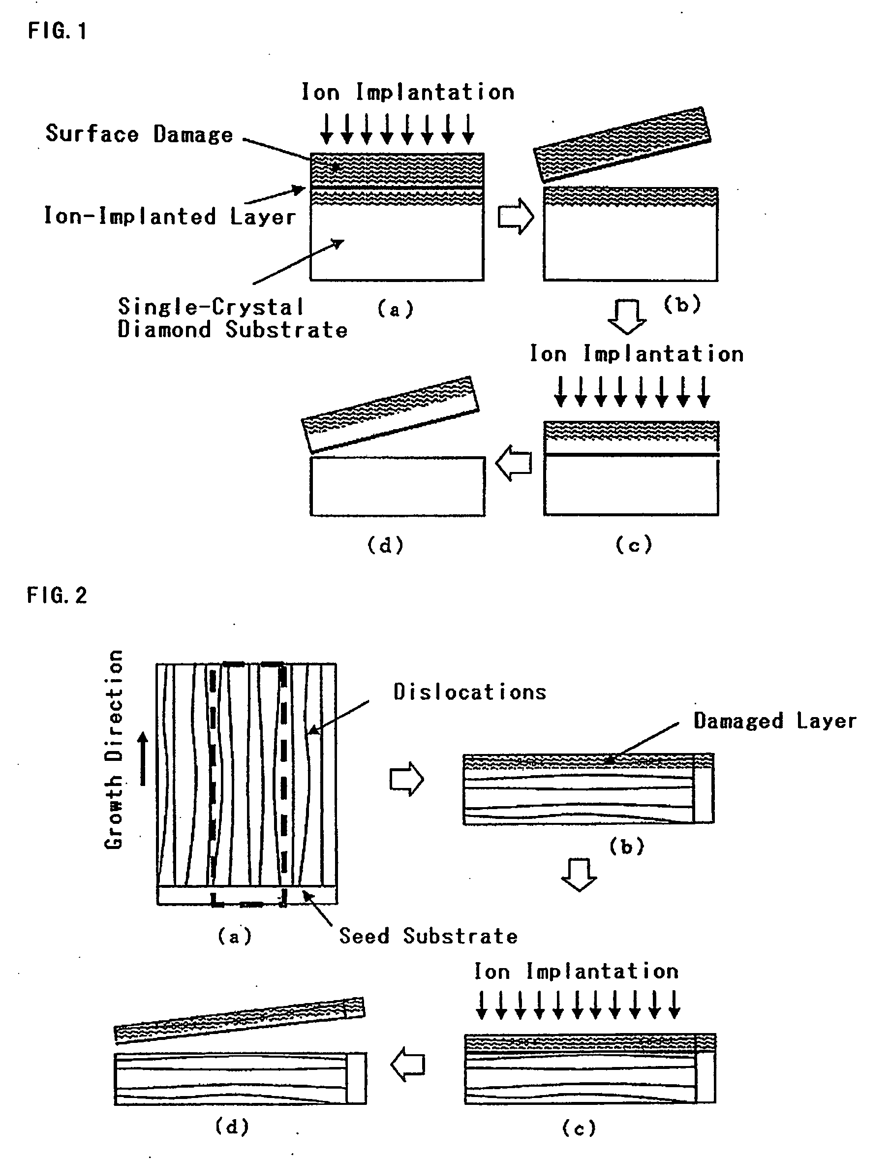
[0070]On an Ib diamond (100) substrate with a size of about 6 x 6 mm synthesized by a high-temperature high-pressure synthesis method, a CVD diamond was grown to a thickness of 8.7 mm by a microwave plasma CVD method. The resulting crystal was cut along the {100} plane in parallel with the growth direction to separate a portion of the crystal, and the surface of the separated crystal was polished to prepare a single-crystal diamond substrate in the form of a 7×8.5×1 mm3 trapezoid. This substrate was observed by transmission X-ray topography to confirm the inclusion of many dislocations toward a direction substantially in parallel with the growth direction.

[0071]According to the same process as in Example 1, the {100} surface of the single-crystal diamond substrate in parallel with the growth direction was subjected to the implantation of carbon ions and heat treatment, growth of a single-crystal diamond film for surface damage evaluation, and removal of a surface layer by electroche...


PUM


Abstract

The present invention provides a process for removing surface damage of a single-crystal diamond, which comprises implanting ions into a single-crystal diamond to form a non-diamond layer near a surface of the diamond, graphitizing the non-diamond layer, and removing a surface layer by etching. According to the invention, the surface damage can be removed or reduced without increasing the surface roughness of a single crystal diamond.

Description

TECHNICAL FIELD[0001]The present invention relates to a surface treatment method for removing or reducing the surface damage of a single-crystal diamond, which is typically used as substrates for electronic devices.BACKGROUND ART[0002]Single-crystal diamond, by virtue of its outstanding semiconductor properties, is expected to be in practical use as a material for electronic devices, such as power devices. In the preparation of such devices, high-quality large single-crystal substrates are required, as with other semiconductor materials.[0003]In the high-temperature high-pressure synthesis method known as the primary synthesis method, the substrate size is considered as limited to about 10×10 mm. In recent years, however, owing to the rapid progression of the single-crystal diamond synthesis technique using a chemical vapor deposition (CVD) method, the synthesis of 10×10 mm substrates, which are equal in size to those synthesized by high-temperature high-pressure synthesis, has been...

Claims


Application Information

Patent Timeline
IPC IPC(8): B44C1/22
CPCH01L21/0405
Inventor MOKUNO, YOSHIAKICHAYAHARA, AKIYOSHIYAMADA, HIDEAKI
Owner NAT INST OF ADVANCED IND SCI & TECH
Why Eureka
Try Eureka