Method and Resulting Structure DRAM Cell with Selected Inverse Narrow Width Effect

Active Publication Date: 2010-01-07
SEMICON MFG INT (SHANGHAI) CORP
View PDF10 Cites 0 Cited by
  • Summary
  • Abstract
  • Description
  • Claims
  • Application Information

AI Technical Summary

Benefits of technology

[0011]Many benefits are achieved by way of the present invention over conventional techniques. For example, the present technique provides an easy to use process that relies upon conventional technology. In some embodiments, the method provides higher device yields in dies per wafer. Additionally, the method provides a process that is compatible with conventional process technology without substantial modifications to conventional equipment and processes. Preferably, the invention provides for improved process integration for design rules of 0.13 microns and less. Additionally, the invention provides isolation structures that may achieve improved electrical characteristics. Preferably, the invention may prevent inverse narrow width effects, commonly called INWE. In certain embodiments, the invention provides for a higher threshold voltage under a small amount of channel dosages. The higher amount of channel dosages in conventional devices causes higher electric fields between a storage node and channel of a dynamic random access memory cell. The higher electric fields are often undesirable. The present invention may achieve lower electric fields between the storage node and channel, which provides improved data retention. Depending upon the embodiment, one or more of these benefits may be achieved. These and other benefits will be described in more throughout the present specification and more particularly below.

Problems solved by technology

An integrated circuit or chip fabrication facility can cost hundreds of millions, or even billions, of U.S. dollars.
Making devices smaller is very challenging, as each process used in integrated fabrication has a limit.
Additionally, as devices require faster and faster designs, process limitations exist with certain conventional processes and materials.
Although there have been significant improvements, such designs still have many limitations.
Additionally, these isolation structures are often difficult to manufacture and generally require complex manufacturing processes and structures.
Furthermore these memory devices often have problems called inverse narrow width effects, commonly known as INWE.

Method used


Image

  • Method and Resulting Structure DRAM Cell with Selected Inverse Narrow Width Effect
  • Method and Resulting Structure DRAM Cell with Selected Inverse Narrow Width Effect
  • Method and Resulting Structure DRAM Cell with Selected Inverse Narrow Width Effect

Examples


Embodiment Construction

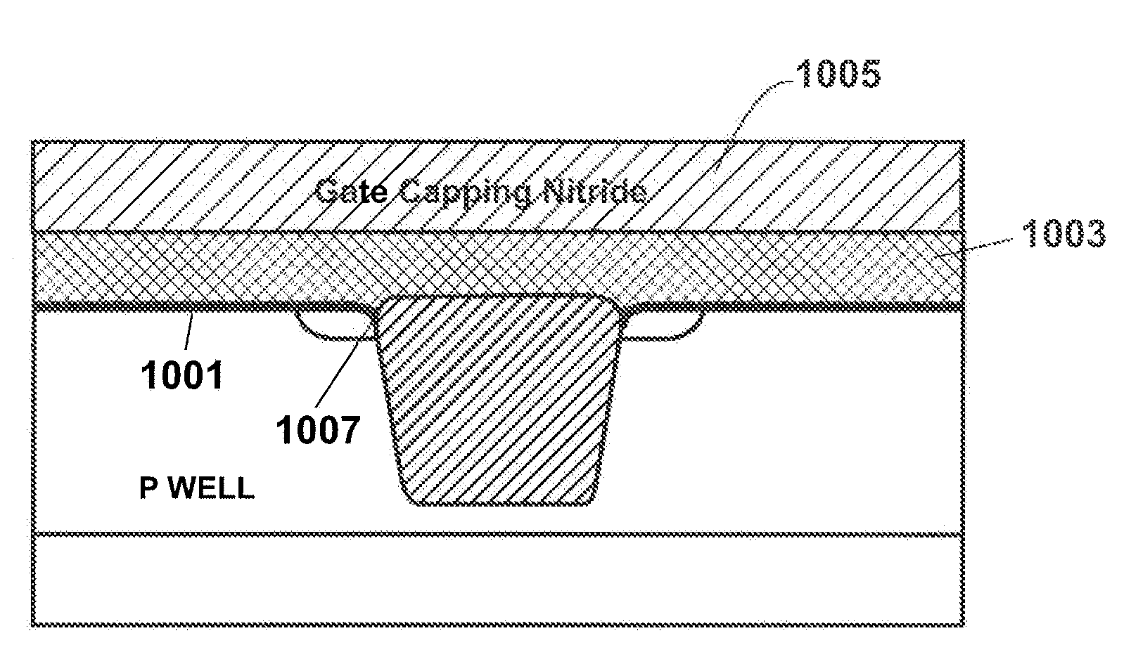
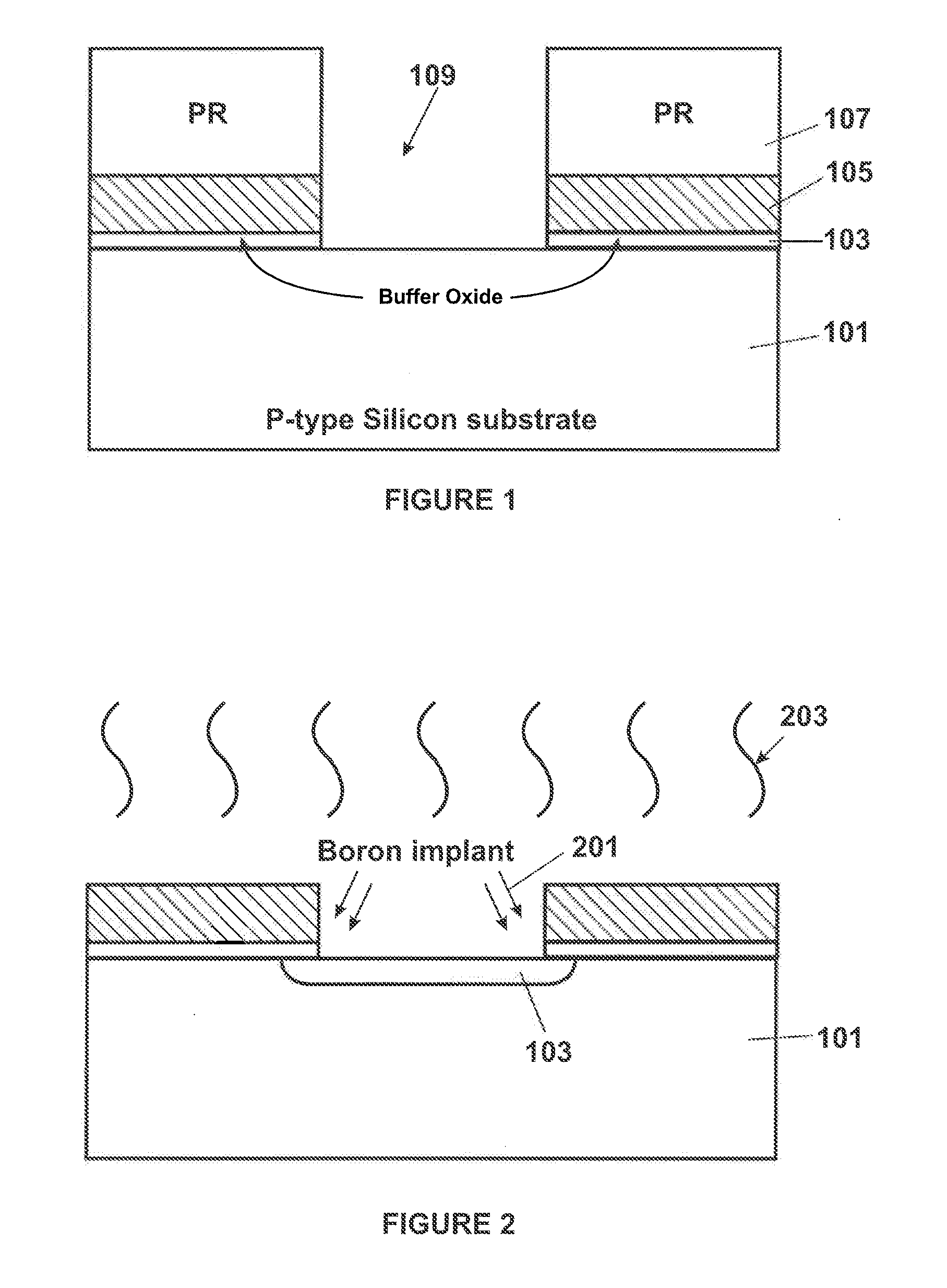
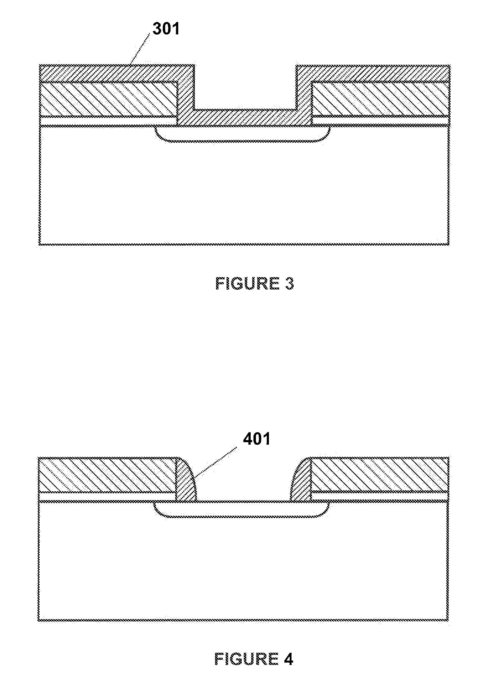
[0016]According to the present invention, techniques for processing integrated circuits for the manufacture of semiconductor devices are provided. More particularly, the invention provides a method and structures for manufacturing an isolation structure for dynamic random access memory devices, commonly called DRAMs. But it would be recognized that the invention has a much broader range of applicability.

[0017]A method for fabricating a shallow trench isolation structure for integrated circuits can be briefly outlined below.

[0018]1. Provide a semiconductor substrate, e.g., silicon wafer;

[0019]2. Form a buffered oxide layer overlying the semiconductor substrate;

[0020]3. Form a pad nitride layer overlying the buffered oxide layer;

[0021]4. Pattern the pad nitride layer to expose a portion of the semiconductor substrate corresponding to a trench region;

[0022]5. Implant P-type material using the patterned pad nitride layer as a masking material at an angle of implanting of less than 45 de...


PUM


Abstract

A shallow trench isolation structure for integrated circuits. The structure includes a semiconductor substrate and a buffered oxide layer overlying the semiconductor substrate. A pad nitride layer is overlying the buffered oxide layer. An implanted region is formed around a perimeter of the trench region. A trench region is formed within the semiconductor substrate. The trench region has a bottom width of less than 0.13 microns and an upper width of less than 0.13 microns. A rounded edge region is within a portion of the semiconductor substrate surrounding a periphery of the trench region. The rounded edges have a radius of curvature greater than about 0.02 um. A planarized high density plasma fill material is formed within the trench region. The structure has a P-well region within the semiconductor substrate and bordering a vicinity of the trench region. A channel region is within the P-well region within the semiconductor substrate. The implanted region has a concentration of more than double an amount of impurities as impurities in the channel region.

Description

CROSS-REFERENCES TO RELATED APPLICATIONS[0001]This application claims priority to Chinese Application No. 200810040296.4, filed Jul. 3, 2008, commonly assigned, and incorporated herein by reference for all purposes.BACKGROUND OF THE INVENTION[0002]The present invention is directed to integrated circuits and their processing for the manufacture of semiconductor devices. More particularly, the invention provides a method and structures for manufacturing an isolation structure for dynamic random access memory devices, commonly called DRAMs. But it would be recognized that the invention has a much broader range of applicability.[0003]Integrated circuits have evolved from a handful of interconnected devices fabricated on a single chip of silicon to millions of devices. Conventional integrated circuits provide performance and complexity far beyond what was originally imagined. In order to achieve improvements in complexity and circuit density (i.e., the number of devices capable of being ...

Claims


Application Information

Patent Timeline
IPC IPC(8): H01L29/00H01L21/76
CPCH01L21/76232H01L21/26513
Inventor YANG, HAE WANG
Owner SEMICON MFG INT (SHANGHAI) CORP
Why Eureka
Try Eureka