

Information recording/reproducing device
a technology of information recording and recording material, which is applied in the field of information recording/reproducing device, can solve the problems of large consumption and inability to realize the new information recording medium using such new recording materials, and achieve the effect of reducing consumption and avoiding the loss of information
- Summary
- Abstract
- Description
- Claims
- Application Information
AI Technical Summary
Benefits of technology
Problems solved by technology
Method used
Image

Examples
first example
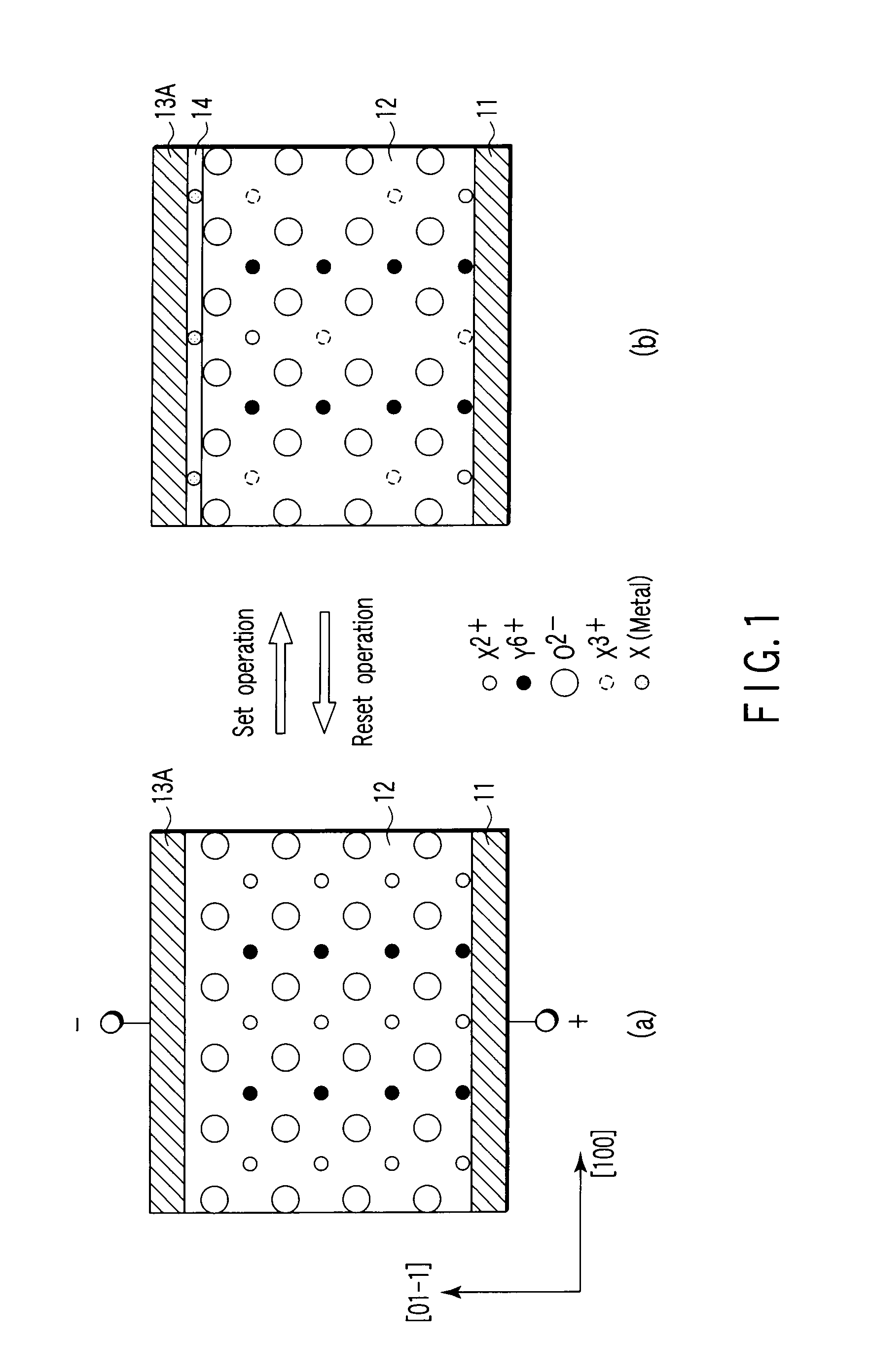
[0188]The first example is a case where the materials of FIG. 1 are used for the recording layer.
[0189]Firstly, as shown in FIG. 7, there is prepared a state where the electric potential of the probe 24 is relatively lower than the electric potential of the electrode layer 21. The probe 24 may be supplied with a negative electric potential, when the electrode layer 21 has a fixed electric potential, for instance, ground potential.
[0190]The current pulse is generated by emitting electrons toward the electrode layer 21 from the probe 24 while using, for instance, an electron generating source or hot electron source. Alternatively, it is also possible to bring the probe 24 into contact with the surface of the recording bit 27 to apply the voltage pulse.
[0191]At this time, for instance, in the recording bit 27 of the recording layer 22, part of X ions moves to the probe (cathode) 24 side, and the number of X ions inside the crystal relatively decreases in comparison to the number of O i...
experiment example
C. Experiment Example
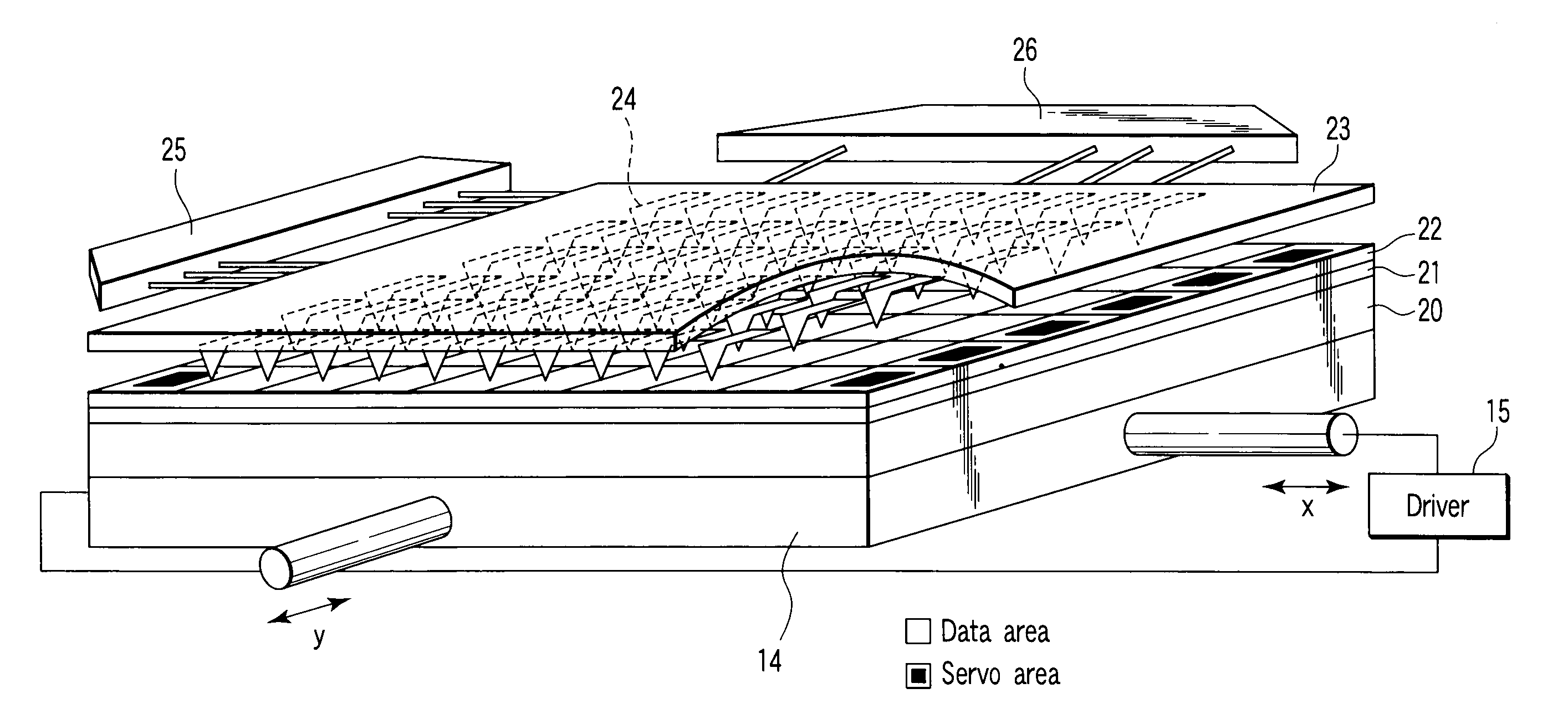
[0212]The recording medium having the structure shown in FIG. 7 is used as a sample, and evaluation may be performed by using a pair of acicular probes whose diameter of a leading edge is 10 nm or less.
[0213]The electrode layer 21 is, for instance, a Pt film formed on a semiconductor substrate. In order to increase adhesion properties between the semiconductor substrate and a lower electrode, Ti of about 5 nm may be used as an adhesion layer. The recording layer 22 can be obtained by performing RF magnetron sputtering on a disk in a mixed gas of argon and oxygen while maintaining the temperature of the disk at a high temperature of about 600° C., by using a target in which components are adjusted so as to have the desired composition. Further, as the protection layer, for instance, diamond-like carbon may be formed by the CVD method. The film thickness of the respective layers can be designed so as to optimize a resistance ratio between the low resistance state ...
experimental example 1
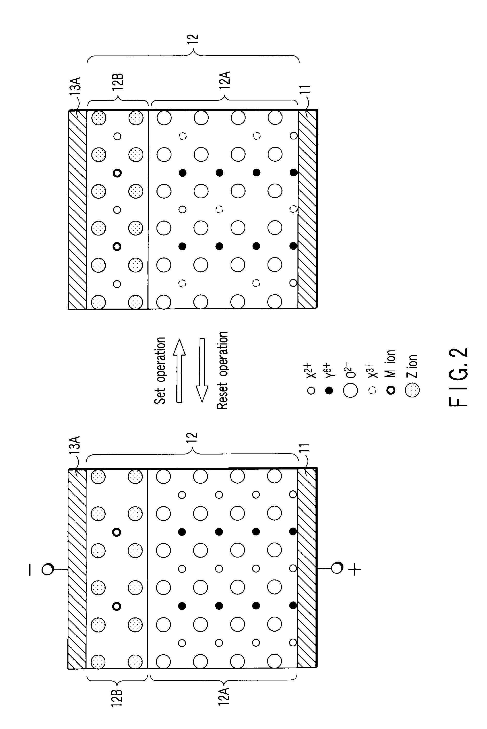
[0218]Shown is an example in which ZrN was used as the buffer layer and NiWO4 was used as the first chemical compound.
[0219]There was performed the film formation of ZrN on the n type (001) Si substrate by using a Zr target (diameter 100 mm). A natural oxide film was previously removed before the film formation. There was obtained ZrN oriented to the orientation of (100), as a result of RF magnetron sputtering, under the condition of RF power 60 W, argon gas 97%, N2 gas 3%, total gas pressure 0.3 Pa, and substrate temperature 500° C. The film thickness of ZrN was made to be 50 nm.
[0220]As the first chemical compound, a film of NiWO4 was formed. The RF magnetron sputtering was performed in the atmosphere of Ar (argon) 95%, and O2 (oxygen) 5%, while using the target in which the mixing ratio of the target was adjusted so as to be a stoichiometric composition at the time the film was formed. RF power was set to 100 W, total gas pressure was set to 1.0 Pa, substrate temperature was set ...
PUM
| Property | Measurement | Unit |
|---|---|---|
| phase change | aaaaa | aaaaa |
| structure | aaaaa | aaaaa |
| chemical | aaaaa | aaaaa |
Abstract
Description
Claims
Application Information