Manufacturing method of semiconductor memory device

a manufacturing method and memory device technology, applied in the direction of semiconductor devices, electrical appliances, basic electric elements, etc., can solve the problems of reducing storage capacity, increasing leakage current, and achieving good data retention properties, good yield

Inactive Publication Date: 2010-01-21
RENESAS ELECTRONICS CORP
View PDF5 Cites 6 Cited by
  • Summary
  • Abstract
  • Description
  • Claims
  • Application Information

AI Technical Summary

Benefits of technology

[0027]The effects obtained by typical embodiments of the inventions disclosed in this application will be briefly described below.
[0028]Since a high-quality amorphous InGeSbTe film can be formed when an InGeSbTe film constituting a memory layer is deposited by the sputtering method, the failure that t

Problems solved by technology

However, the DRAM which stores information depending on the amount of charge accumulated in a capacitor has a problem that the storage capacity is reduced if the area of the capacitor is decreased.
There is also a problem that the leakage current is increased if a dielectric material of the capacitor is thinned below a predetermined value.
Up un

Method used


Image

  • Manufacturing method of semiconductor memory device
  • Manufacturing method of semiconductor memory device
  • Manufacturing method of semiconductor memory device

Examples


Embodiment Construction

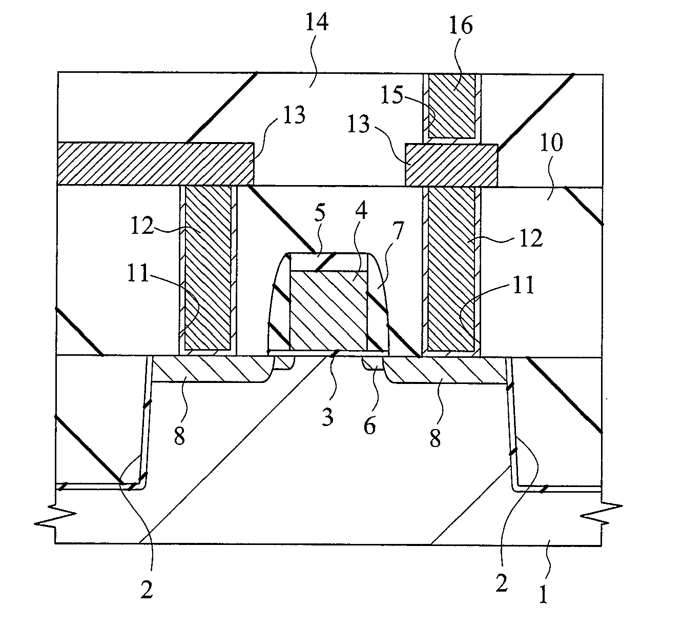
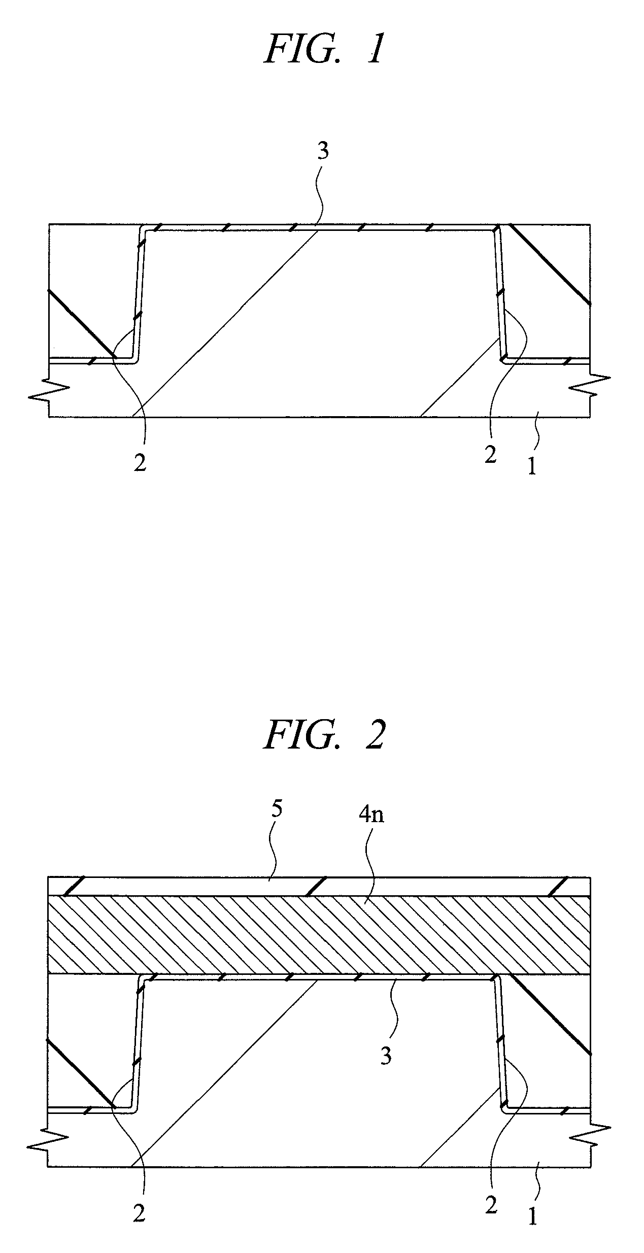
[0049]Hereinafter, embodiments of the present invention will be described in detail with reference to the accompanying drawings. Note that components having the same function are denoted by the same reference numbers throughout the drawings for describing the embodiments, and the repetitive description thereof will be omitted. Also, the composition formula for the three-component chalcogenide made of Ge, Sb and Te of the present invention is GexSbyTez, and when the composition ratios x, y and z are arbitrary, the composition formula is expressed as GeSbTe in an abbreviated manner in some cases. Further, the same is true of the four or more component chalcogenide. For example, the composition formula for the four-component chalcogenide made of Ge, Sb, Te and In is InwGexSbyTez, and when the composition ratios x, y, z and w are arbitrary, the composition formula is expressed as InGeSbTe in an abbreviated manner in some cases.

[0050]The manufacturing method of a phase change memory acco...


PUM


Abstract

In a step of forming an InGeSbTe film which contains GeSbTe made of germanium (Ge), antimony (Sb) and tellurium (Te) as its base material and to which indium (In) is added, an InGeSbTe film is formed by sputtering on a semiconductor substrate while keeping a temperature of the semiconductor substrate between an in-situ crystallization temperature of GeSbTe serving as the base material and an in-situ crystallization temperature of InGeSbTe. As a result, it is possible to suppress the failure that the phase separation occurs in the InGeSbTe film during the following manufacturing process.

Description

TECHNICAL FIELD[0001]The present invention relates to a manufacturing technique of a semiconductor memory device, and more particularly to a technique effectively applied to the manufacture of a phase change memory using a chalcogenide film for a memory layer.BACKGROUND ART[0002]Information devices, electric home appliances, in-vehicle devices and others are mounted with a microcomputer for an embedded device, in which a flash memory for storing a program and data is embedded (memory-embedded microcomputer). In recent years, with the improvement in performance of these devices, the demands for improving the performance of the memory-embedded microcomputer have been increasing, and further improvement in the rewriting durability and the integration degree of the embedded flash memory has been demanded.[0003]Furthermore, also in the DRAM which is a general-purpose memory, in order to satisfy the demand for higher integration, scaling-down of the memory cells has been advanced. However...

Claims


Application Information

Patent Timeline
IPC IPC(8): H01L21/00H01L21/06
CPCH01L45/06H01L45/12H01L45/1233H01L27/2436H01L45/1625H01L45/1675H01L45/144H10B63/30H10N70/231H10N70/801H10N70/826H10N70/8828H10N70/026H10N70/063
Inventor MATSUI, YUICHIMORIKAWA, TAKAHIRO
Owner RENESAS ELECTRONICS CORP
Why Eureka
Try Eureka