Image sensor with reduced red light crosstalk

Inactive Publication Date: 2010-02-04
EASTMAN KODAK CO
View PDF12 Cites 32 Cited by
  • Summary
  • Abstract
  • Description
  • Claims
  • Application Information

AI Technical Summary

Benefits of technology

[0015]An image sensor in accordance with the invention may be advantageously implemented in a digital camera or other type of imag

Problems solved by technology

However, the presence of metallization level interconnects and various other features associated with the dielectric layers on the frontside of the image sensor can adversely impact the fill factor and quantum efficiency of the image sensor.
A prob

Method used


Image

  • Image sensor with reduced red light crosstalk
  • Image sensor with reduced red light crosstalk
  • Image sensor with reduced red light crosstalk

Examples


Example

[0021]The present invention will be illustrated herein in conjunction with particular embodiments of digital cameras, image sensors, and processing techniques for forming such image sensors. It should be understood, however, that these illustrative arrangements are presented by way of example only, and should not be viewed as limiting the scope of the invention in any way. Those skilled in the art will recognize that the disclosed arrangements can be adapted in a straightforward manner for use with a wide variety of other types of imaging devices and image sensors.

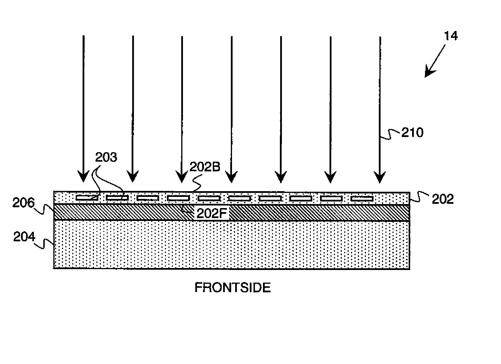
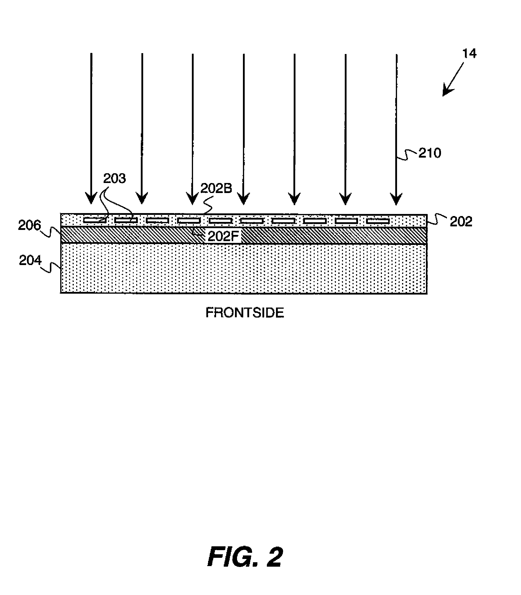
[0022]For example, although the image sensors of certain of the illustrative embodiments described herein are configured for backside illumination, other embodiments may be configured for frontside illumination, and the present invention is not limited in this regard. Also, embodiments of the invention may be implemented as stacked image sensors, SOT image sensors, or in other configurations.

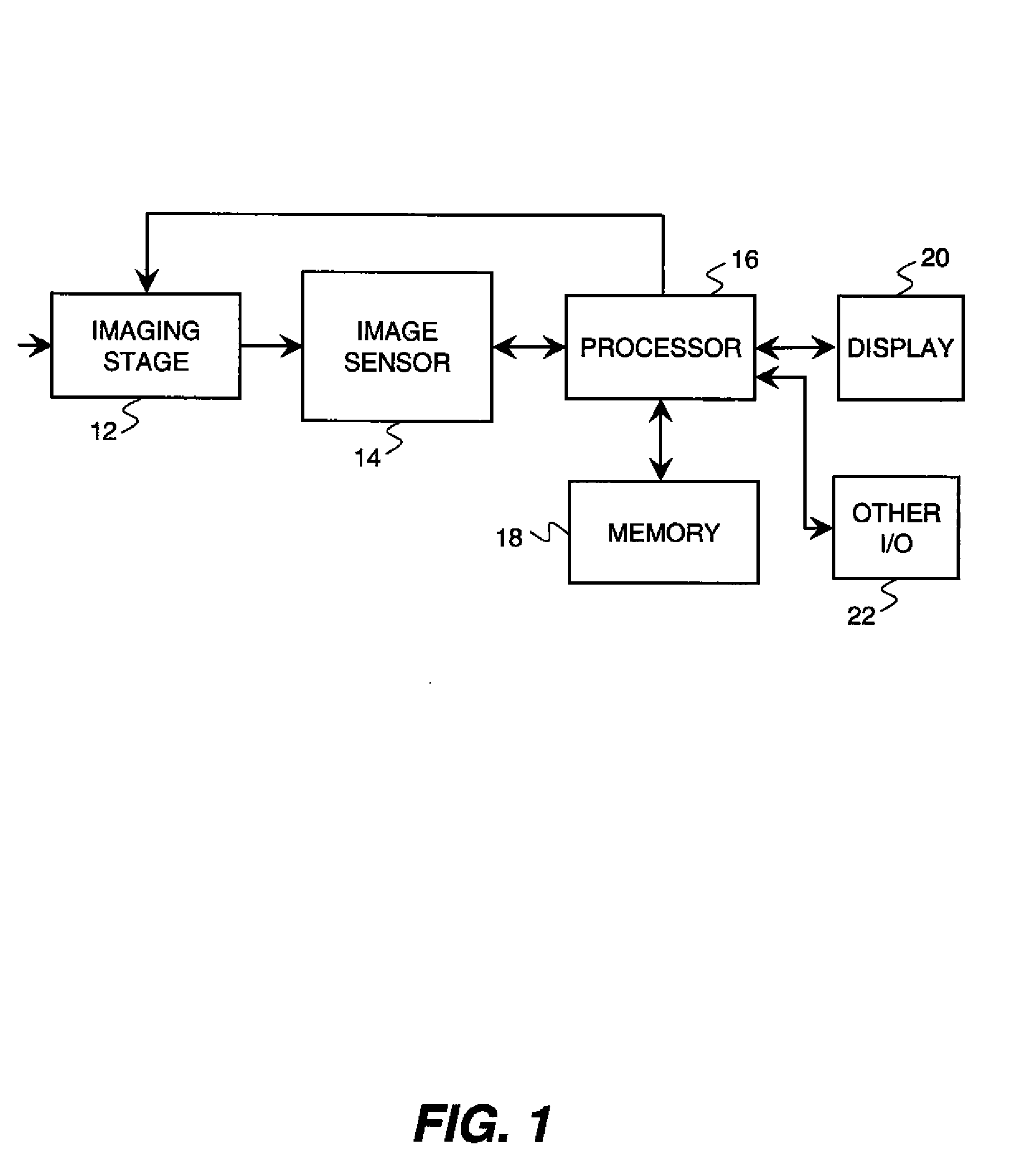
[0023]FIG. 1 shows a digital ca...


PUM


Abstract

An image sensor having a pixel array includes a sensor layer comprising a plurality of photosensitive elements of the pixel array, a circuit layer comprising circuitry associated with the pixel array, and a crosstalk reduction layer arranged between the sensor layer and the circuit layer and configured to reduce crosstalk between adjacent ones of the photosensitive elements. The crosstalk reduction layer may comprise, for example, an amorphous silicon germanium (a-SiGe) layer specifically configured to reduce red light crosstalk in the image sensor. The image sensor may be implemented in a digital camera or other type of digital imaging device.

Description

FIELD OF THE INVENTION[0001]The present invention relates generally to electronic image sensors for use in digital cameras and other types of imaging devices, and more particularly to processing techniques for use in forming image sensors.BACKGROUND OF THE INVENTION[0002]A typical electronic image sensor comprises a number of light sensitive picture elements (“pixels”) arranged in a two-dimensional array. Such an image sensor may be configured to produce a color image by forming an appropriate color filter array (CFA) over the pixels. Examples of image sensors of this type are disclosed in U.S. Patent Application Publication No. 2007 / 0024931, entitled “Image Sensor with Improved Light Sensitivity,” which is incorporated by reference herein.[0003]As is well known, an image sensor may be implemented using complementary metal-oxide-semiconductor (CMOS) circuitry. In such an arrangement, each pixel typically comprises a photodiode and other circuitry elements that are formed in a silico...

Claims


Application Information

Patent Timeline
IPC IPC(8): H04N5/228G03G15/00
CPCH01L27/14623H01L27/14625H01L27/14632H01L27/14634H01L27/14689H01L27/1464H01L27/14692H01L31/02164H01L31/0232H01L31/03765H01L27/1469
Inventor CHEN, SHENLIN
Owner EASTMAN KODAK CO
Why Eureka
Try Eureka