Laminated device

a laminated inductors and laminate technology, applied in the direction of magnetic materials, inductances, magnetic bodies, etc., can solve the problems of unsuitable lamination, low electric resistance, and several problems of laminated inductors, and achieve excellent dc superposition characteristics, stable characteristics, and reduced internal-electrode-induced residual stress

Active Publication Date: 2010-02-11
HITACHI METALS LTD
View PDF7 Cites 43 Cited by
  • Summary
  • Abstract
  • Description
  • Claims
  • Application Information

AI Technical Summary

Benefits of technology

[0010]Accordingly, an object of the present invention is to provide a laminated device having stable characteristics such as inductance, a Q value, etc., and excellent DC superposition characteristics, with internal-electrode-induced residual stress reduced, and delamination and cracking suppressed.DISCLOSURE OF THE INVENTION
[0016]Because the non-magnetic ceramic layer has a different linear thermal expansion coefficient from that of the conductor pattern, stress distribution change by the formation of the non-magnetic ceramic layer should be taken into consideration. As a result of intensive investigation, it has been found that when a non-magnetic ceramic layer is formed inside both peripheries of the conductor patterns, stress is concentrated in peripheral portions of the non-magnetic ceramic layer, resulting in a reduced effect of stress relaxation. The concentration of stress can be avoided by extending both peripheries of the non-magnetic ceramic layer from both peripheries of the conductor patterns in a plane direction such that the peripheries of the conductor patterns are sufficiently separate from the peripheries of the non-magnetic ceramic layer, thereby preventing the cracking of the magnetic ferrite layers. The conductor patterns are preferably sandwiched by the non-magnetic ceramic layers, such that the conductor patterns are positioned substantially at a plane-direction center of the non-magnetic ceramic layers adjacent in a lamination direction.

Problems solved by technology

Mn—Zn ferrite is known as soft ferrite having high Bs, but its low electric resistance makes it unsuitable for lamination.
The laminated inductors suffer several problems.
The first problem is that the magnetic permeability of ferrite changes when strain is added.
As a result, the laminated inductor has uneven performance and low reliability.
However, it has been found that the formation of void layers is not sufficient for stress relaxation, and that voids lower the strength of the laminated inductor.
In addition, a gas generated during eliminating the carbon paste causes the delamination (peeling of layers) of the laminated inductor and the cracking of ferrite.
The delamination and cracking are likely to permit a plating liquid, etc. to intrude into the laminated inductor, causing the short-circuiting of conductor patterns.
In addition, because the non-magnetic, insulating layers reach an outer surface of this inductor, a plating liquid, etc. are likely to intrude into the inductor through cracks and delaminated portions in interfaces between the magnetic layers and the non-magnetic insulating layers, causing the short-circuiting of conductor patterns.

Method used


Image

  • Laminated device
  • Laminated device
  • Laminated device

Examples


first embodiment

[1] First Embodiment

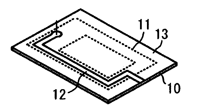
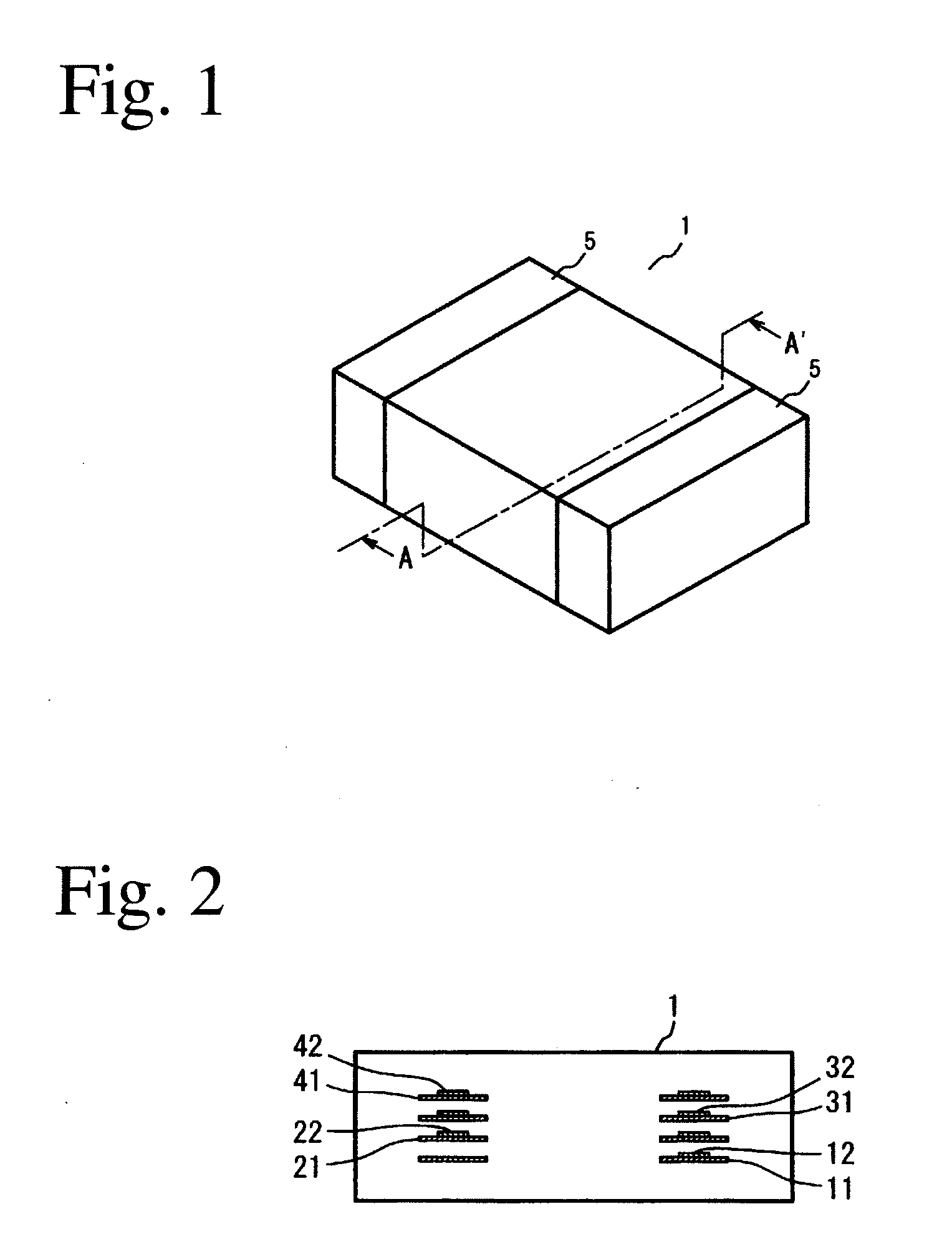
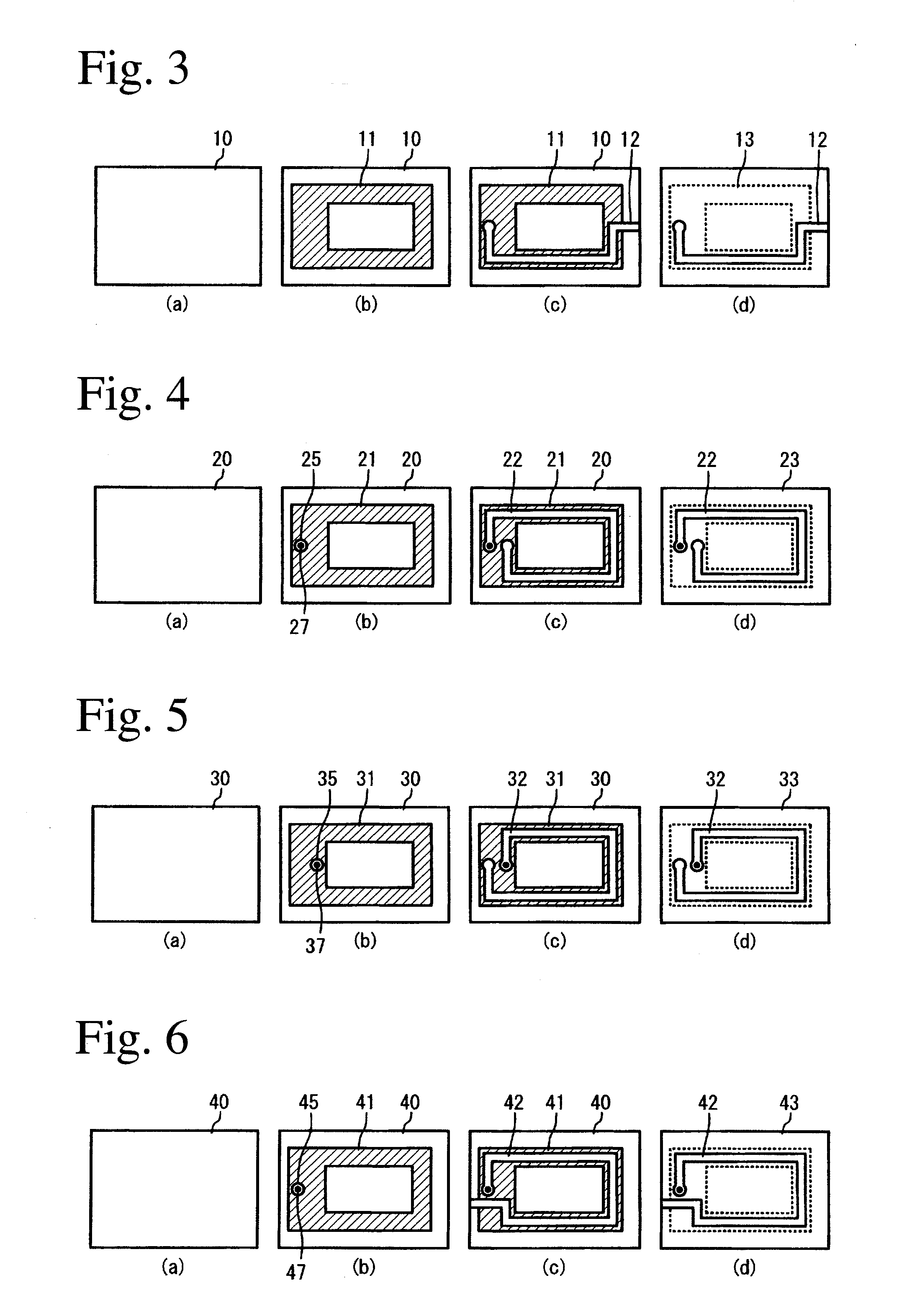
[0056]FIG. 1 shows the appearance of the laminated inductor according to the first embodiment of the present invention, FIG. 2 is a cross-sectional view taken along the line A-A′ in FIG. 1, and FIGS. 3-7 show its production steps. The laminated inductor in this embodiment comprises a coil embedded in a ferrite laminate, both ends of the coil being connected to external electrodes 5 formed on a laminate surface by baking a conductive paste of Ag, etc. As shown in FIG. 2, non-magnetic ceramic layers 11, 21, 31, 41 are in contact with coil-constituting conductor patterns 12, 22, 32, 42. The conductive paste for forming external electrodes is not particularly restricted, but may be, for instance, an Ag alloy containing at least one of Pt, Pd, Au, Cu and Ni, etc.

[0057]The magnetic ferrite layer is made of, for instance, a ferrite composition comprising Fe2O3, ZnO and NiO, part of which may be substituted by CuO, as main components. The main component composition prefe...

second embodiment

[2] Second Embodiment

[0077]FIG. 8 shows the cross section (corresponding to the cross section taken along the line A-A′ in FIG. 1) of the laminated inductor in the second embodiment, and FIGS. 9 to 18 show its production steps. Because the laminated inductor in the second embodiment has the same portions as in the first embodiment, only different portions will be explained in detail below.

[0078]In the laminated inductor in this embodiment, non-magnetic ceramic layers 101, 121, 141, 161, 181 are formed between coil-constituting conductor patterns 112, 132, 152, 172. The conductor patterns 112, 132, 152, 172 and the non-magnetic ceramic layers 101, 121, 141, 161, 181 are formed on different magnetic ferrite sheets 100, 110, 120, 130, 140, 150, 160, 170, 180. The conductor patterns are connected through via-holes 127, 137, 147, 157, 167, 177 formed in the magnetic ferrite sheets 120, 140, 160 each provided with a non-magnetic ceramic layer, and in the magnetic ferrite sheets 130, 150, ...

third embodiment

[3] Third Embodiment

[0081]FIG. 19 shows the cross section (corresponding to the cross section taken along the line A-A′ in FIG. 1) of the laminated inductor in the third embodiment, and FIG. 20 shows its production steps. In this embodiment, the non-magnetic ceramic layers are formed on an entire coil-covering region (including a region inside the coil). Because the non-magnetic ceramic layers act as magnetic gaps for a magnetic flux in a region inside the coil, the DC superposition characteristics are improved, resulting in high inductance at high frequencies. With respect to other points, the laminated inductor in this embodiment does not differ from that in the first embodiment.


PUM

PropertyMeasurementUnit
BET specific surface areaaaaaaaaaaa
thicknessaaaaaaaaaa
BET specific surface areaaaaaaaaaaa

Abstract

A laminated device comprising pluralities of magnetic ferrite layers, conductor patterns each formed on each magnetic ferrite layer and connected in a lamination direction to form a coil, and a non-magnetic ceramic layer formed on at least one magnetic ferrite layer such that it overlaps the conductor patterns in a lamination direction, the non-magnetic ceramic layer comprising as main components non-magnetic ceramics having higher sintering temperatures than that of the magnetic ferrite, and further one or more of Cu, Zn and Bi in the form of an oxide.

Description

FIELD OF THE INVENTION[0001]The present invention relates to a laminated device such as a coil-containing laminated inductor, etc., particularly to a laminated device having excellent characteristics and reduced internal stress free from delamination and cracking.BACKGROUND OF THE INVENTION[0002]As power supply circuits for small electronic appliances such as cell phones, portable information terminals (PDA), note-type personal computers, digital cameras, etc., switching regulators (DC-DC converters) suffering less power loss in voltage conversion are widely used. Passive elements such as inductors, capacitors, etc. used in DC-DC converter circuits should be made smaller to reduce an area occupied by the power supply circuit.[0003]Because the switching frequencies of DC-DC converters have been increased to improve their power efficiency and performance, inductors and capacitors contained in them have smaller constants, making it possible to miniaturize these parts. Thus, the inducto...

Claims


Application Information

Patent Timeline
Patent Type & Authority Applications(United States)
IPC IPC(8): H01F5/00
CPCH01F17/0013H01F3/14B32B18/00C04B35/265C04B2235/3208C04B2235/3232C04B2235/3239C04B2235/3251C04B2235/3274C04B2235/3277C04B2235/3279C04B2235/3281C04B2235/3284C04B2235/3293C04B2235/3298C04B2235/3418C04B2235/5409C04B2235/5436C04B2235/5445C04B2235/6025C04B2235/72C04B2237/34C04B2237/341C04B2237/343C04B2237/348C04B2237/704H01F41/046H01F17/04H01F17/00
Inventor KATAYAMA, YASUHISAUMENO, TOHRUTACHIBANA, TAKESHI
Owner HITACHI METALS LTD
Why Eureka
Try Eureka