Semiconductor light-emitting device, manufacturing method thereof, and lamp

Active Publication Date: 2010-03-04
TOYODA GOSEI CO LTD
View PDF5 Cites 16 Cited by
  • Summary
  • Abstract
  • Description
  • Claims
  • Application Information

AI Technical Summary

Benefits of technology

[0041]According to the semiconductor light-emitting device of the present invention, a semiconductor light-emitting device having excellent light extraction efficiency and low wavelength unevenness can be obtained by forming a random concavo-convex surface on at least a part of the surface of the titanium oxide-b

Problems solved by technology

However, in the light-emitting device described in Patent Document 1, since the semiconductor material is treated, the semiconductor layer is subjected to loading and is thus damaged.
Therefore, although the light extraction efficiency is improved, the internal quantum efficiency is lowered, causing a problem in that the emission intensity can not be increased.
However, since the refractive index of ITO is as small as 1.9, as compared to 2.6 for the GaN-based compound semiconductor, total reflection occurs at the interface between the ITO and the GaN-based compound semiconductor, which causes

Method used


Image

  • Semiconductor light-emitting device, manufacturing method thereof, and lamp
  • Semiconductor light-emitting device, manufacturing method thereof, and lamp
  • Semiconductor light-emitting device, manufacturing method thereof, and lamp

Examples


experimental example 1

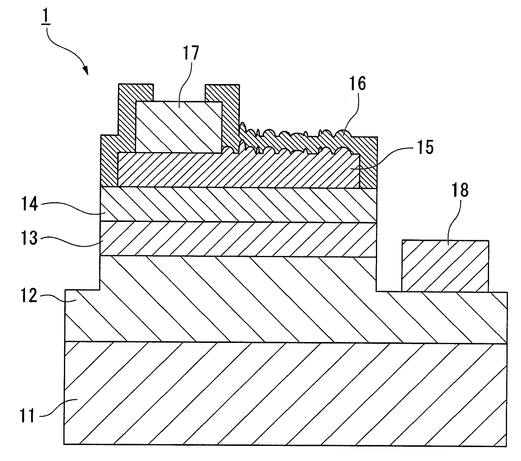
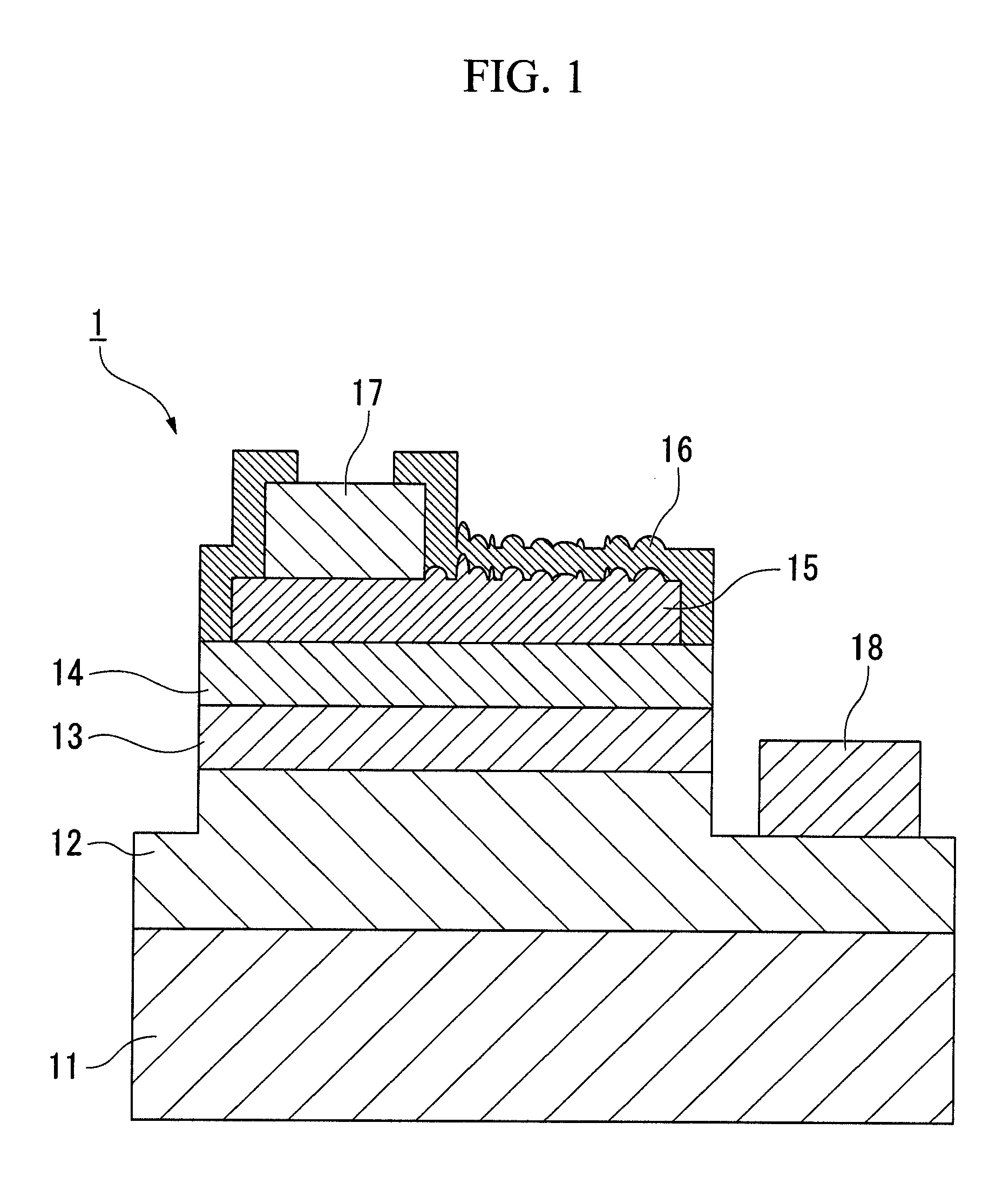
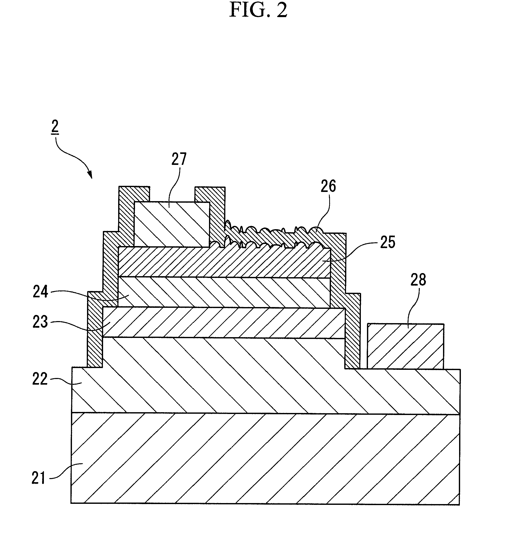
[0189]FIG. 2 shows a cross-sectional schematic diagram of a gallium nitride-based compound semiconductor light-emitting device produced in the present Experimental Example. FIG. 5 shows a planar schematic diagram thereof.

(Production of Gallium Nitride-Based Compound Semiconductor Light-Emitting Device)

[0190]On a substrate 21 made of sapphire was laminated a gallium nitride-based compound semiconductor layer via a buffer layer made of AlN. This gallium nitride-based compound semiconductor layer comprised:

[0191]an n-type semiconductor layer 22 in which an under layer of undoped GaN in a thickness of 8 μm, a Ge-doped n-type GaN-contact layer in a thickness of 2 μm, and an n-type In0.1Ga0.9N-clad layer in a thickness of 0.02 μm were laminated in this order;

[0192]a light-emitting layer 23 of a multiple quantum well structure obtained by five laminations of a Si-doped GaN barrier layer in a thickness of 16 nm and an In0.06Ga0.94N well layer in a thickness of 2.5 nm with a barrier layer on...


PUM


Abstract

There is provided a semiconductor light-emitting device having excellent light extraction efficiency and low wavelength unevenness, a manufacturing method thereof, and a lamp. A semiconductor light-emitting device includes an n-type semiconductor layer 12, a light-emitting layer 13, a p-type semiconductor layer 14, and a titanium oxide-based conductive film layer 15 laminated in this order, wherein a random concavo-convex surface 15 is formed on at least a part of the surface of the titanium oxide-based conductive film layer.

Description

BACKGROUND OF THE INVENTION[0001]1. Field of the Invention[0002]The present invention relates to a semiconductor light-emitting device, and particularly to a semiconductor light-emitting device having excellent light extraction efficiency, a manufacturing method thereof, and a lamp.[0003]2. Description of Related Art[0004]In recent years, gallium nitride (GaN)-based compound semiconductor materials, which are nitride-based semiconductors, have become of interest as a semiconductor material for producing a light-emitting device that emits light of short wavelength. A GaN-based compound semiconductor is grown on a substrate of sapphire single crystal, a variety of oxides, or a Group III-V compound, through a metal-organic chemical vapor deposition method (MOCVD method), a molecular-beam epitaxy method (MBE method), or the like.[0005]As a structure of a general GaN-based compound semiconductor light-emitting device, if a sapphire single crystal substrate is employed, an n-type semicond...

Claims


Application Information

Patent Timeline
IPC IPC(8): H01L33/00
CPCH01L33/32H01L2933/0091H01L33/44H01L33/42H01L2224/48091H01L2224/48247H01L2224/48257
Inventor OSAWA, HIROSHIFUKUNAGA, NAOKISHINOHARA, HIRONAO
Owner TOYODA GOSEI CO LTD
Why Eureka
Try Eureka