Atomic composition controlled ruthenium alloy film formed by plasma-enhanced atomic layer deposition

Active Publication Date: 2010-03-04
ASM JAPAN
View PDF98 Cites 41 Cited by
  • Summary
  • Abstract
  • Description
  • Claims
  • Application Information

AI Technical Summary

Benefits of technology

[0015]In view of the above, the inventors examined combinations of Ta material and Ru material. In particular, the inventors examined materials that can be broken down by H2 plasma or H2/N2 plasma. Furthermore, the inventors examined an optimal composition in the depth direction of a film made by these materials, and a method for controlling such composition, in order to ensure adhesion and barrier property of the film as a Cu wiring liner. In an embodiment of a method for forming a RuTaN film being a Cu barrier film, combining Ta material with H2/N2 plasma, and Ru material with H2/N2 plasma, is effective. A stable RuTaN film can be formed by increasing the flow rate ratio of N2 or adjusting the H2/N2 plasma time. If H2 plasma is applied after the supply of Ta material, the residual carbon content in the film increases, thereby resulting in lower density and higher resistance. When H2/N2 plasma is applied, on the other hand, the resistance becomes lower and the residual carbon content decreases. Accordingly, it is effective to use plasma of H2/N2 mixed gas after the supply of Ta material. In the meantime, in an embodiment a RuTa film containing less N can be formed by combining Ta material with H2/N2 plasma, and Ru material with H2 plasma. In this case, the resistivity can be lowered by reducing the N content, and also stable resistivity can be achieved acco

Problems solved by technology

On the other hand, it has been confirmed that a TaN film formed by the atomic layer deposition method would result in lower adhesion with Cu wiring.
This makes it more difficult, than under the PVD method, to ensure good adhesion when a TaN film or TaNC film is formed as a Cu barrier metal.
If the adhesion of Cu with this Cu barrier metal is poor, however, the Cu film will separate in the reliability test and voids will be formed.
However, traditionally forming a Ru film was difficult over the exposed areas of Cu wiring at the bottom of via holes because normally the adhesion is poor at the interface between inter-layer insulation film and Ru.
However, the prior arts mentioned above are associated with at least the problems explained below.
However, use of NH3 plasma or H2/N2 plasma promotes nitriding of the Ta layer formed as the bottom layer, resulting in significantly high film resistivity.
Accordingly, applying the present invention to via holes connecting the top-layer Cu wiring layer and bottom-layer Cu wiring, which is the object of the aforementioned publi

Method used


Image

  • Atomic composition controlled ruthenium alloy film formed by plasma-enhanced atomic layer deposition
  • Atomic composition controlled ruthenium alloy film formed by plasma-enhanced atomic layer deposition
  • Atomic composition controlled ruthenium alloy film formed by plasma-enhanced atomic layer deposition

Examples


Example

EXAMPLE 1

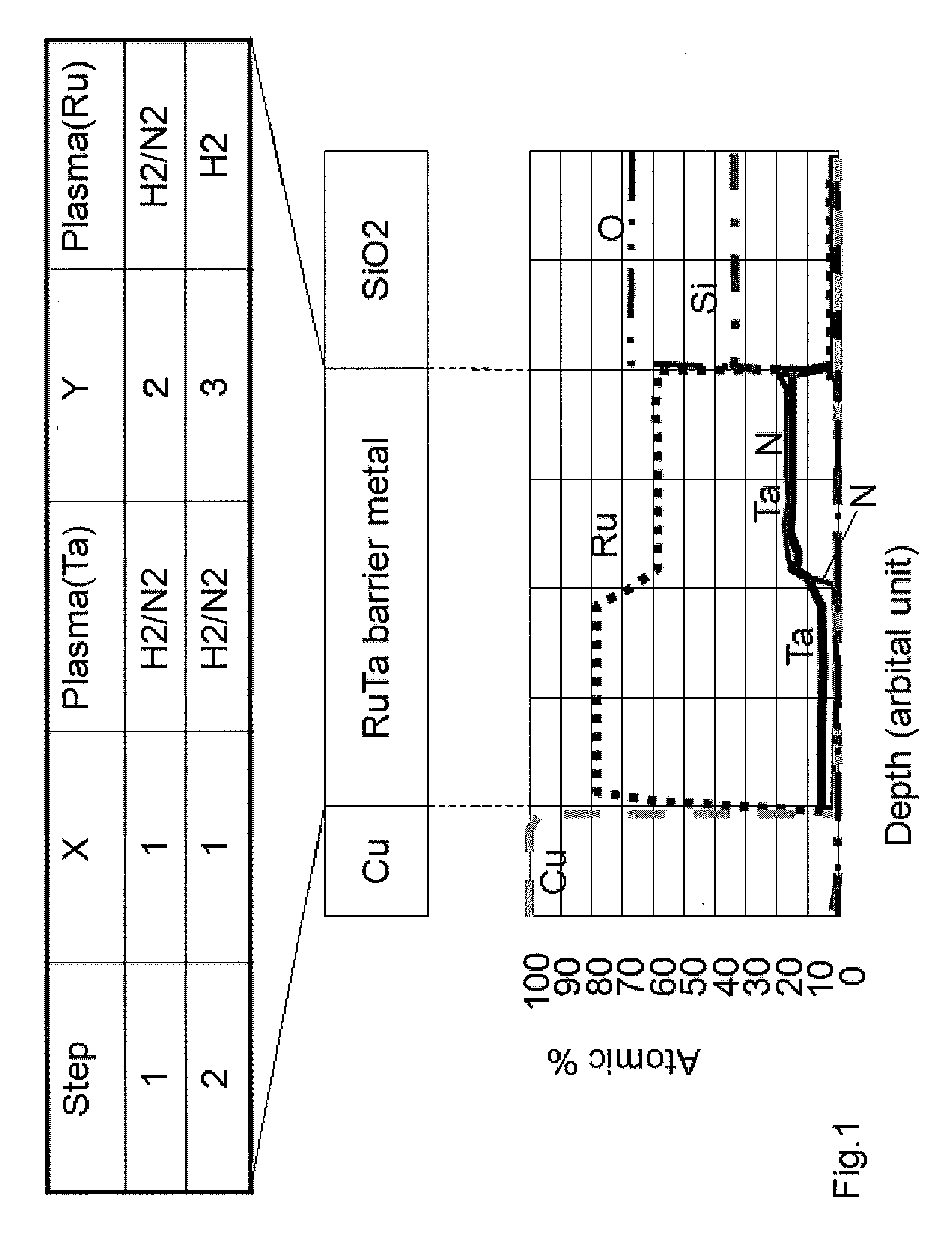
[0204]A specific example where the process in FIG. 1 is implemented using the apparatus shown in FIG. 4 based on the process sequences shown in FIGS. 5 and 6 is explained.

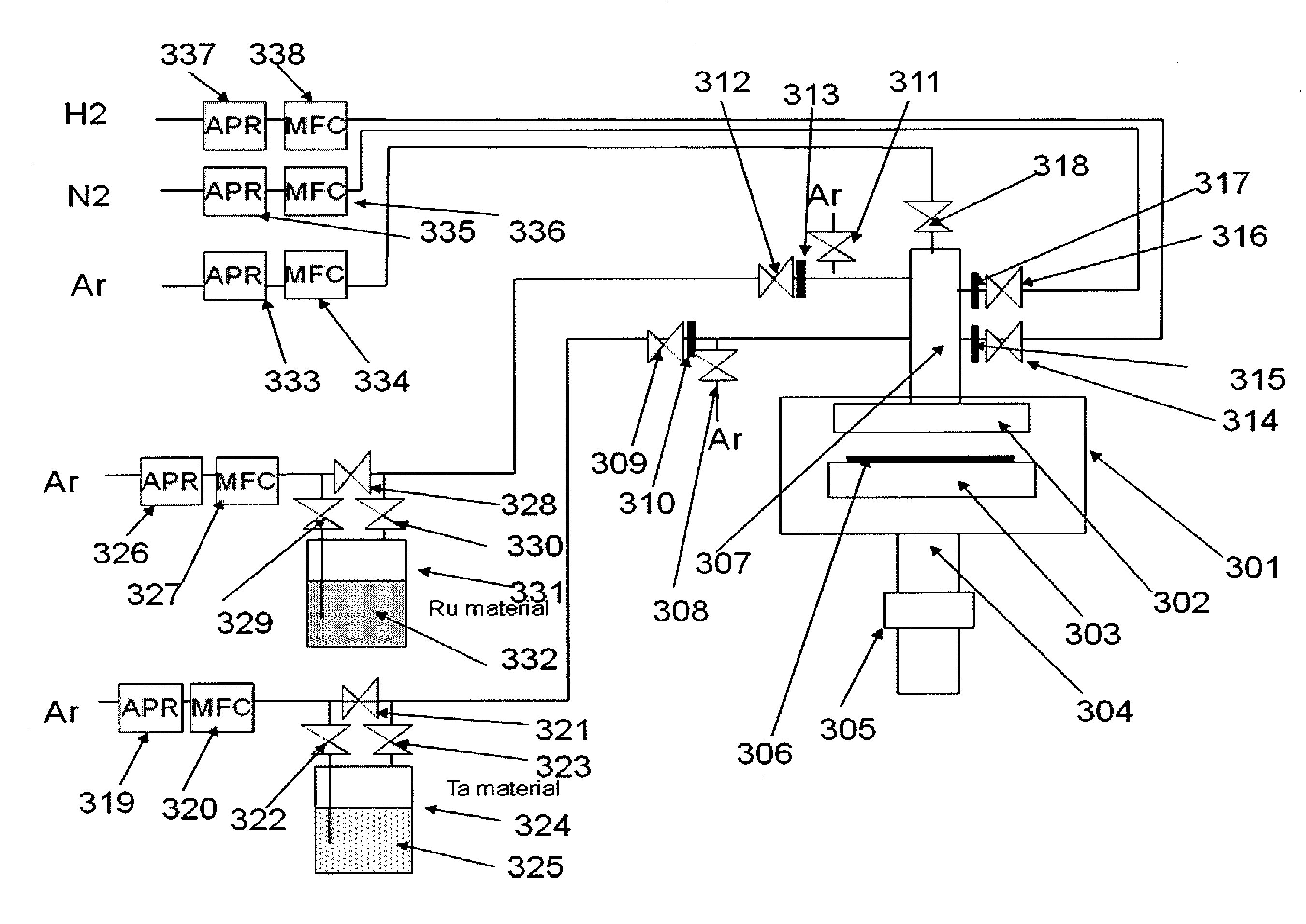
[0205]A Cu wiring is formed according to the process shown in FIG. 7 in a Cu wiring forming process based on dual damascene structure. Silicon substrates having a device that has been processed up to the state in FIG. 7(a) are treated using the apparatus shown in FIG. 10. A silicon substrate is set in a cassette loader 501, and a transfer robot 502 is used to transfer the substrate into a load lock chamber 503, after which the substrate is transferred by a vacuum robot 504 from the load lock chamber 503 into a reaction chamber for plasma atomic layer deposition 505. The next substrate is transferred to a reaction chamber 507, and the subsequent substrate is transferred to a reaction chamber 508, to allow the process to be implemented in a similar manner. The substrate transferred to the reaction chamber 5...

Example

EXAMPLE 2

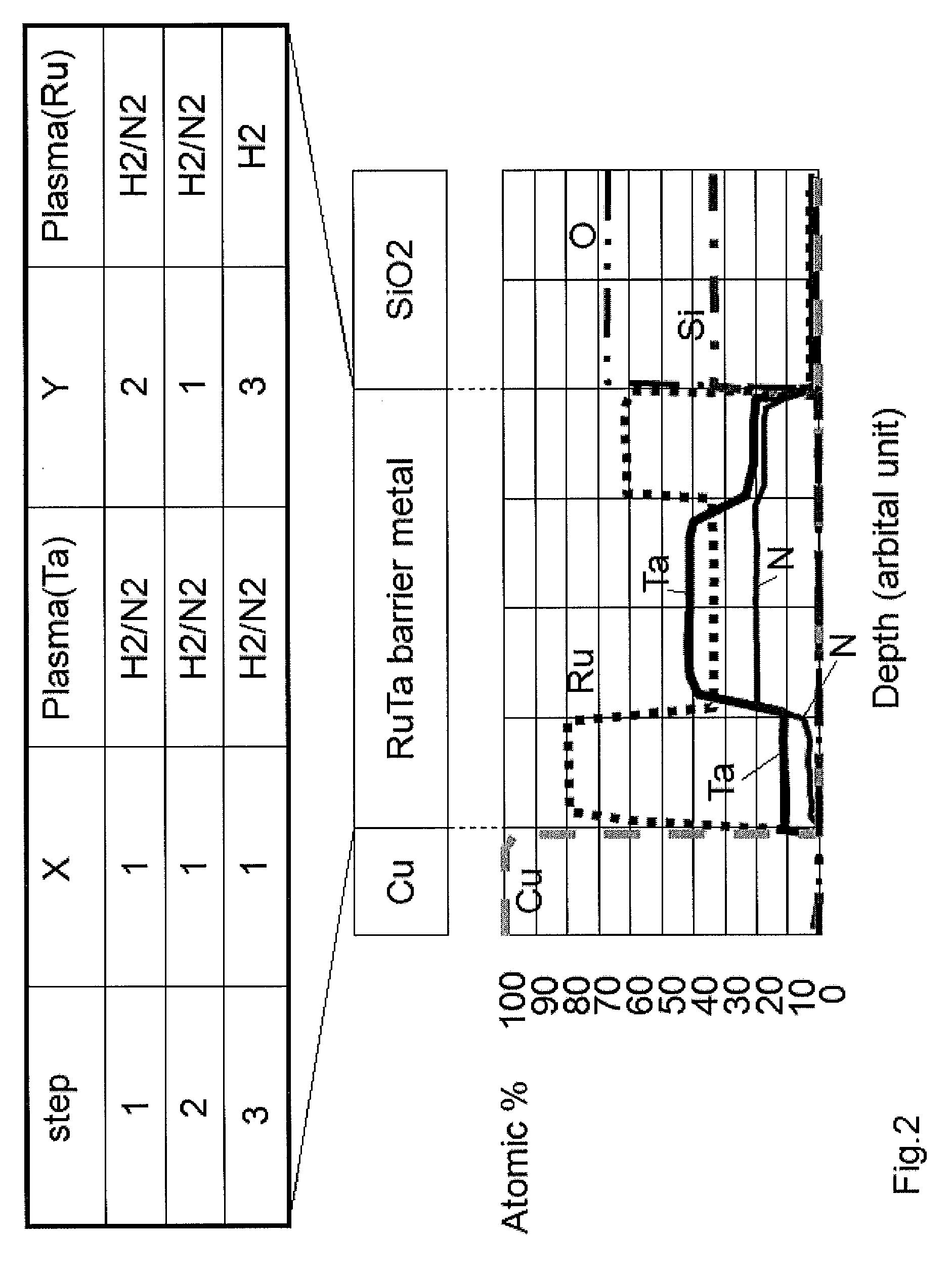
[0209]A specific example where the process in FIG. 2 is implemented using the apparatus shown in FIG. 4 based on the process sequences shown in FIGS. 5 and 6 is explained.

[0210]A Cu wiring is formed according to the process shown in FIG. 8 in a Cu wiring forming process based on dual damascene structure. Silicon substrates having a device that has been processed up to the state in FIG. 8(a) are treated using the apparatus shown in FIG. 10. A silicon substrate is set in a cassette loader 501, and a transfer robot 502 is used to transfer the substrate into a load lock chamber 503, after which the substrate is transferred by a vacuum robot 504 from the load lock chamber 503 into a reaction chamber for plasma atomic layer deposition 505. The next substrate is transferred to a reaction chamber 507, and the subsequent substrate is transferred to a reaction chamber 508, to allow the process to be implemented in a similar manner. The substrate transferred to the reaction chamber 5...

Example

EXAMPLE 3

[0213]A specific example where the process in FIG. 1 is implemented using the apparatus shown in FIG. 4 based on the process sequences shown in FIGS. 5 and 6 is explained.

[0214]A Cu wiring is formed according to the process shown in FIG. 9 in a Cu wiring forming process based on dual damascene structure. Silicon substrates having a device that has been processed up to the state in FIG. 9(a) are treated using the apparatus shown in FIG. 10. A silicon substrate is set in a cassette loader 501, and a transfer robot 502 is used to transfer the substrate into a load lock chamber 503, after which the substrate is transferred by a vacuum robot 504 from the load lock chamber 503 into a reaction chamber for plasma atomic layer deposition 505. The next substrate is transferred to a reaction chamber 507, and the subsequent substrate is transferred to a reaction chamber 508, to allow the process to be implemented in a similar manner. The substrate transferred to the reaction chamber 5...


PUM

PropertyMeasurementUnit
Thicknessaaaaaaaaaa
Thicknessaaaaaaaaaa
Thicknessaaaaaaaaaa

Abstract

A metal film composed of multiple atomic layers continuously formed by atomic layer deposition of Ru and Ta or Ti includes at least a top section and a bottom section, wherein an atomic composition of Ru, Ta or Ti, and N varies in a thickness direction of the metal film. The atomic composition of Ru, Ta or Ti, and N in the top section is represented as Ru(x1)Ta/Ti(y1)N(z1) wherein an atomic ratio of Ru(x1)/(Ta/Ti(y1)) is no less than 15, and z1 is 0.05 or less. The atomic composition of Ru, Ta or Ti, and N in the bottom section is represented as Ru(x2)Ta/Ti(y2)N(z2) wherein an atomic ratio of Ru(x2)/(Ta/Ti(y2)) is more than zero but less than 15, and z2 is 0.10 or greater.

Description

BACKGROUND [0001]1. Field of the Invention[0002]The present invention relates to a method for forming a Cu diffusion barrier metal for metal wiring structures that can be favorably used in the creation of fine semiconductor elements in general, as well as a structure of such Cu diffusion barrier metal.[0003]2. Description of the Related Art[0004]Ru film is drawing the attention for its property to improve the adhesion with Cu, when a Ru film is formed at the interface between Cu and barrier metal in a Cu wiring structure which is the main wiring structure used in high-speed logic elements such as MPUs, and thereby significantly enhance the reliability of wiring. Methods are being studied to form a Ru film that provides a Cu wiring liner on a TaN film or WN film and then form a Cu film on top of the Ru film (one example of such method relating to a combination of Ru and TaN is described in C. C. Yong et al., “Physical, Electrical, and Reliability Characterization of Ru for Cu Interco...

Claims


Application Information

Patent Timeline
IPC IPC(8): B32B9/00B32B5/00
CPCC23C16/34C23C16/4554H01L21/28562H01L21/76846H01L2924/0002H01L23/53238H01L2924/00
Inventor SHINRIKI, HIROSHINAMBA, KUNITOSHIJEONG, DAEKYUN
Owner ASM JAPAN
Why Eureka
Try Eureka