Resistance change element and semiconductor device including the same

a technology of resistance change element and memory element, which is applied in the direction of semiconductor devices, bulk negative resistance effect devices, electrical appliances, etc., can solve the problems of different performance requirements for resistance change element when it is used as a memory element, and it is difficult to miniaturize even a semiconductor transistor which does not have charge accumulation function, etc., to achieve low resistance and high off resistance

Active Publication Date: 2010-03-11
NEC CORP
View PDF2 Cites 23 Cited by
  • Summary
  • Abstract
  • Description
  • Claims
  • Application Information

AI Technical Summary

Benefits of technology

[0021]The present invention can provide a resistance change element that achieves high OFF resistance while maintaining low ON resistance. The resistance change element according to the present invention can be used not only as a memory element but also as a switching element.

Problems solved by technology

Although miniaturization is essential to increase the capacity, it has been difficult to miniaturize even a semiconductor transistor which does not have charge accumulation function.
However, the performance required for a resistance change element when it is used as a memory element is different from that required when it is used as a switch that connects wiring lines.

Method used


Image

  • Resistance change element and semiconductor device including the same
  • Resistance change element and semiconductor device including the same
  • Resistance change element and semiconductor device including the same

Examples


first exemplary embodiment

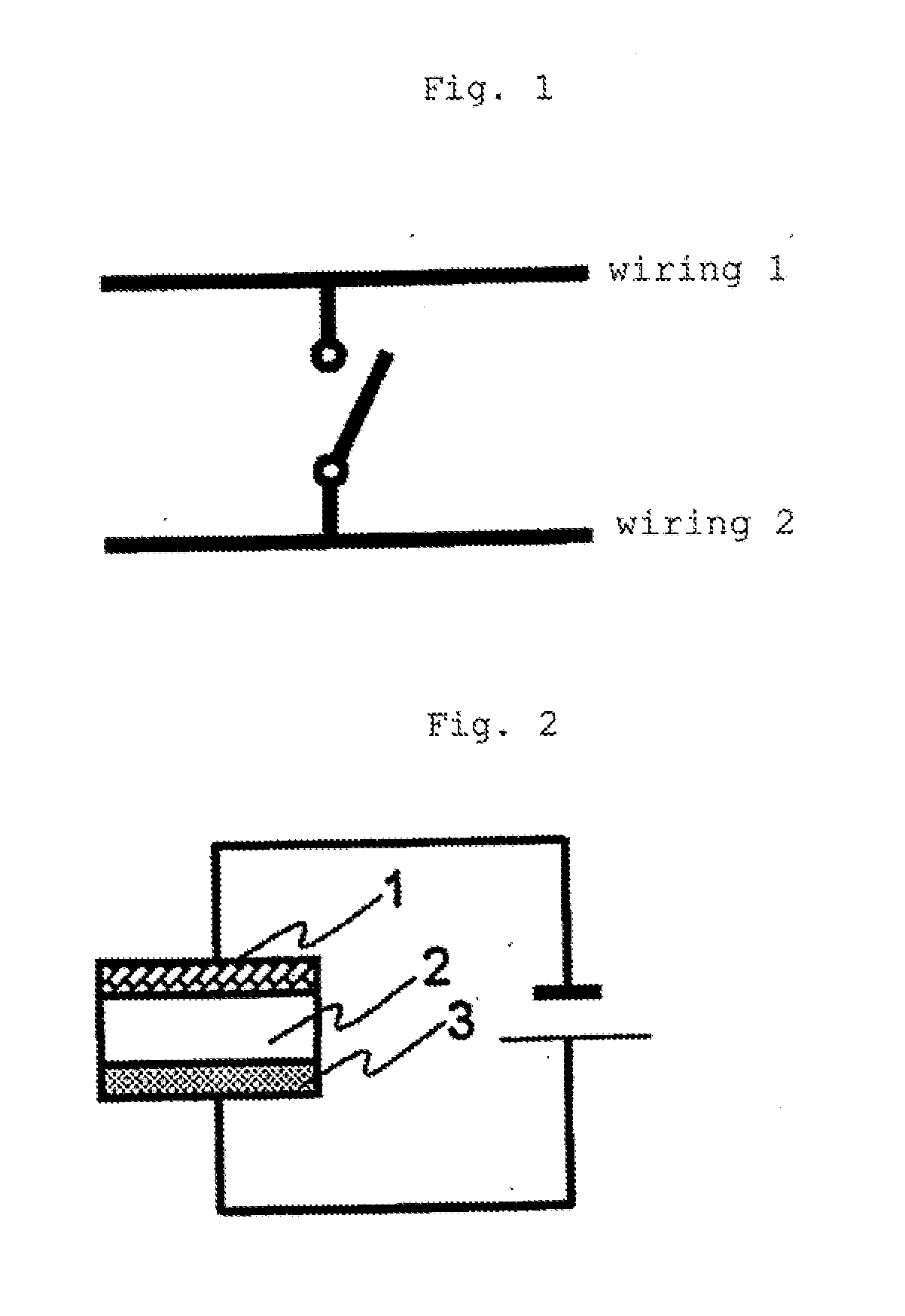
[0061]FIG. 7 shows the current-voltage characteristic in the ON state and the OFF state when 10 mol % of Ta was added to nickel oxide (NiO). The upper and lower electrodes were made of Ru.

[0062]The upper and lower electrodes and the resistance change film were formed by sputtering in the present experiment. In particular, the resistance change film was formed by using a sintered target made of NiO to which Ta was added. The film thickness was approximately 80 nm. The lower electrode and the resistance change film were not processed, but the upper electrode was shaped into a circle having a diameter of 100 μm.

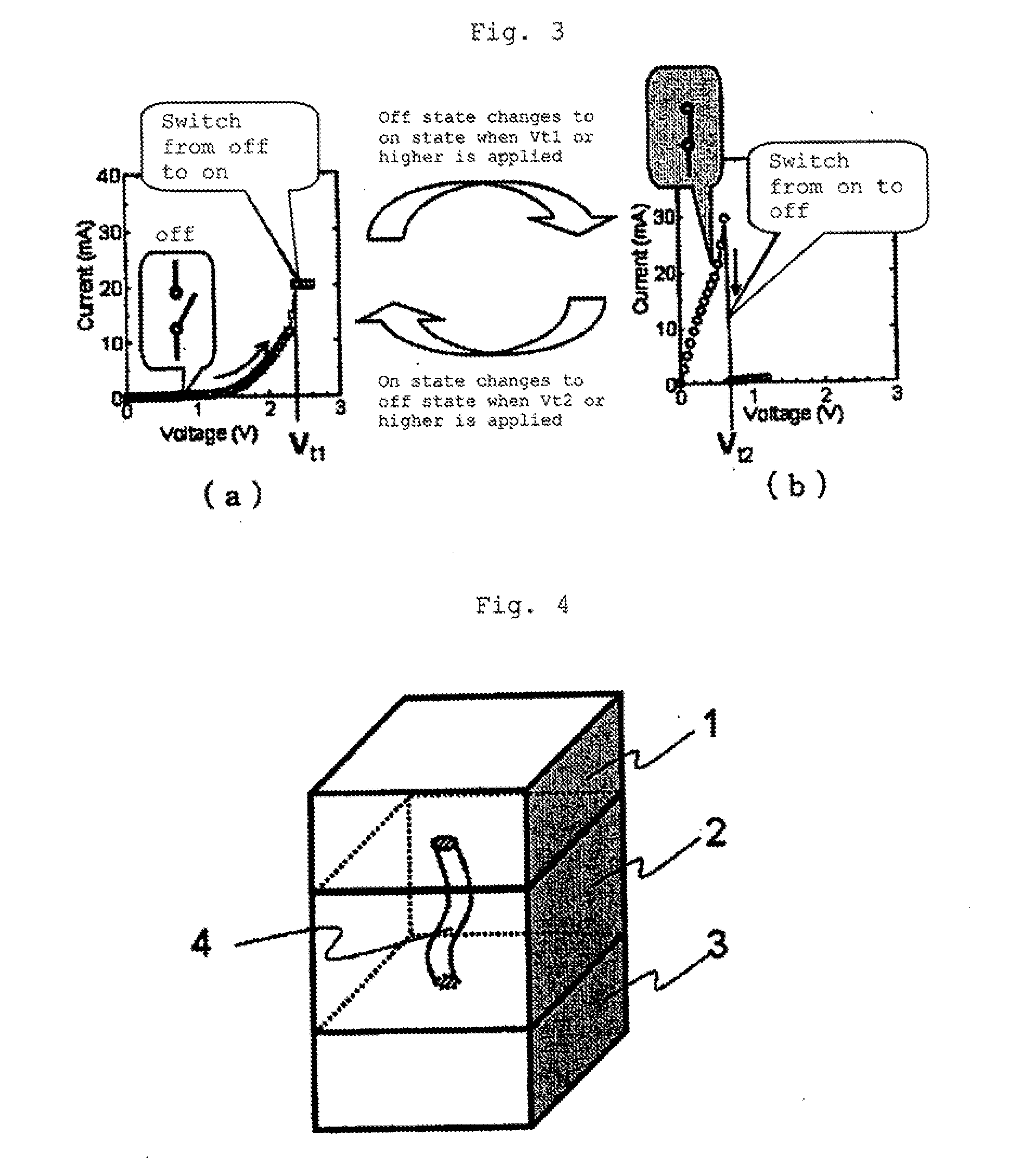
[0063]The characteristic indicated by the dashed lines is the current-voltage characteristic of the resistance change element made of NiO to which no Ta was added. FIG. 7 indicates that the current-voltage characteristic in the ON state remains unchanged irrespective of whether or not Ta was added, but adding Ta can increase the OFF resistance by at least triple digits, for exam...

second exemplary embodiment

[0064]While the present invention is significant for a switch that controls interconnection between wiring lines, the present invention may be applied to a memory element connected in series to a semiconductor transistor, a diode, or any other active element. When the present invention is applied to a memory element and when the difference between the ON resistance and the OFF resistance is large, high performance, for example, a short readout time, can be achieved.

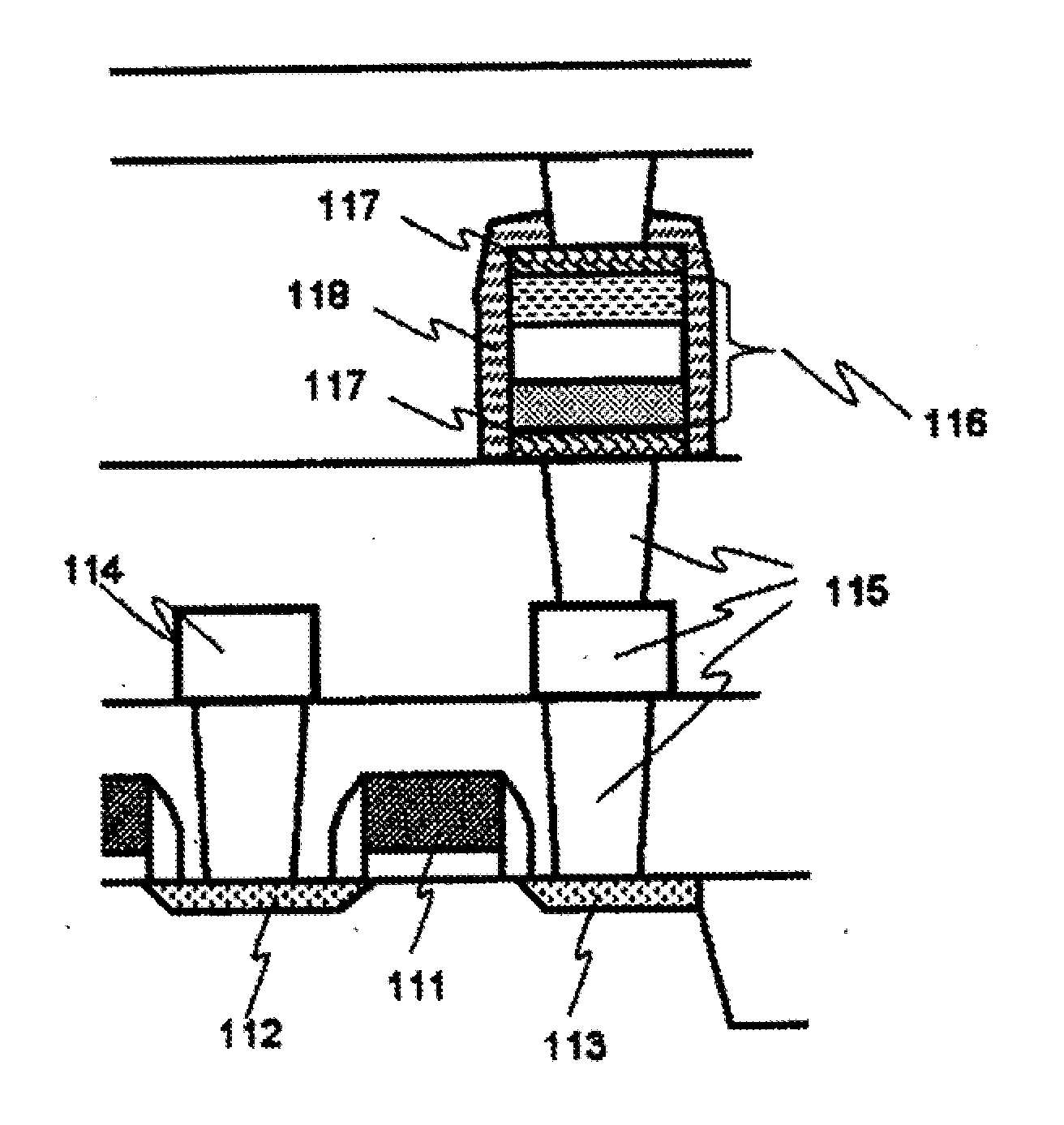
[0065]FIG. 8 shows an exemplary embodiment of a semiconductor storage device having a configuration in which the resistance change element of the present invention is formed on a semiconductor transistor. A semiconductor substrate made of silicon (Si) or any other suitable element is first prepared. A transistor is formed on the semiconductor substrate, and a wiring line 115 made of W, Al, Cu, or any other suitable element is formed on the drain 113 of the transistor in such a way that the wiring line 115 extends upward a...


PUM


Abstract

To use a resistance change element having an MIM structure, which is obtained by stacking a metal, a metal oxide, and a metal, as a switching element, it is necessary to achieve OFF resistance higher than that required in a memory element by a factor of at least 1000. On the other hand, when a resistance change element is used as a memory element and when the difference between the ON resistance and the OFF resistance is a large value, high performance, for example, a short readout time, can be achieved. The present invention therefore provides a resistance change element capable of maintaining low ON resistance and achieving high OFF resistance. High OFF resistance can be achieved while low ON resistance is maintained by adding a second metal that is not contained in a metal oxide, which is a resistance change material, the second metal being capable of charge-compensating for metal deficiency or oxygen deficiency.

Description

FIELD OF THE INVENTION[0001]The present invention relates to a resistance change element that can be used as a nonvolatile memory element or a switching element, and a semiconductor device including the resistance change element.DESCRIPTION OF THE RELATED ART[0002]As represented by flash memories and SONOS (silicon oxide nitride oxide semiconductor) memories, nonvolatile memories currently dominating the market are achieved by using a technique that make use of electric charges accumulated in an insulating film disposed above the channel to change the threshold voltage of a semiconductor transistor. Although miniaturization is essential to increase the capacity, it has been difficult to miniaturize even a semiconductor transistor which does not have charge accumulation function. To address the problem, studies have been conducted to further increase capacity by allowing a transistor to have only a switching function of selecting a memory cell to and from which data is written and re...

Claims


Application Information

Patent Timeline
Patent Type & Authority Applications(United States)
IPC IPC(8): H01L47/00
CPCH01L27/101H01L45/04H01L27/2436H01L45/146H01L45/1625H01L45/1233H10B63/30H10N70/20H10N70/026H10N70/8833H10N70/826
Inventor ITO, KIMIHIKOSUNAMURA, HIROSHIYABE, YUKO
Owner NEC CORP
Why Eureka
Try Eureka