Chip for surface plasmon resonance sensor and surface plasmon resonance sensor

a technology of surface plasmon and sensor, which is applied in the direction of optical radiation measurement, instruments, spectrometry/spectrophotometry/monochromator, etc., can solve the problems of increasing the size of the apparatus, and affecting the accuracy of the apparatus, so as to achieve the effect of small size and high accuracy

Inactive Publication Date: 2010-03-18
ORMON CORP
View PDF5 Cites 21 Cited by
  • Summary
  • Abstract
  • Description
  • Claims
  • Application Information

AI Technical Summary

Benefits of technology

[0014]The present invention was made in view of the aforementioned circumstances and aims at providing a surface plasmon resonance sensor and a surface plasmon resonance sensor chip having small sizes and high accuracy which are capable of dispersing the light of signals from a sample detection portion having a plurality of dielectric layers with different thicknesses (hereinafter, light reflected by the sample detection portion may be referred to as signals) for detecting the conditions of the surfaces of respective determination areas.

Problems solved by technology

However, presently, these apparatuses have large sizes and are expensive and, in order to increase the processing efficiency for enabling performing a plurality of inspections at one time or in order to increase the determination accuracy, it has been necessary to increase the sizes of these apparatuses and to make these apparatuses more expensive.
However, such inspection apparatuses induce the problem of the occurrence of errors due to fluorescent coloring agents, since they detect imperceptible fluorescence, and also induce the problem of large sizes of optical systems for fluorescence detection and, therefore, high fabrication costs.
Such a bulk-type surface plasmon resonance sensor induces no error due to fluorescent molecules, but its structure is difficult to array and, accordingly, only a single inspection can be performed at one time with a single surface plasmon resonance sensor.
Furthermore, conventional bulk-type surface plasmon resonance sensors have involved image processing for analyses, which has caused the surface plasmon resonance sensors to have large sizes and also has required times for analyses.
The structure having a single core enables providing only a single metal thin film therein, which makes it impossible to perform a plurality of inspections at one time.
Accordingly, such a surface plasmon resonance sensor having a plurality of cores has had the problem of the necessity of significantly increasing the size of the sensor in order to enable performing a plurality of inspections.

Method used


Image

  • Chip for surface plasmon resonance sensor and surface plasmon resonance sensor
  • Chip for surface plasmon resonance sensor and surface plasmon resonance sensor
  • Chip for surface plasmon resonance sensor and surface plasmon resonance sensor

Examples


first example

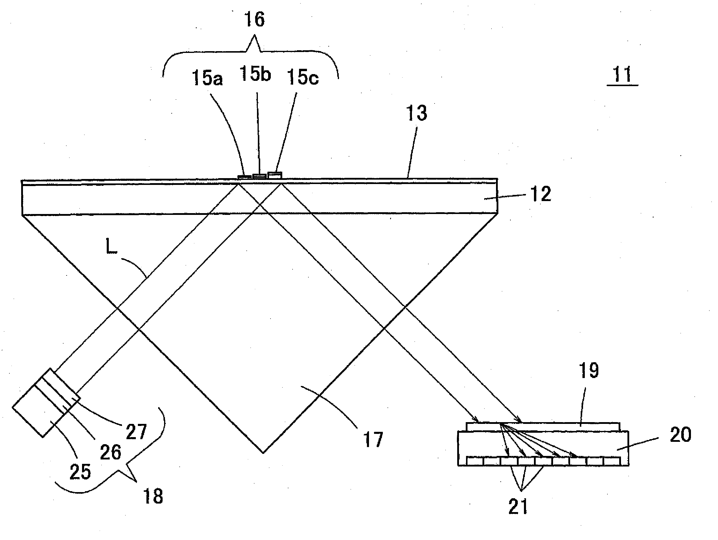
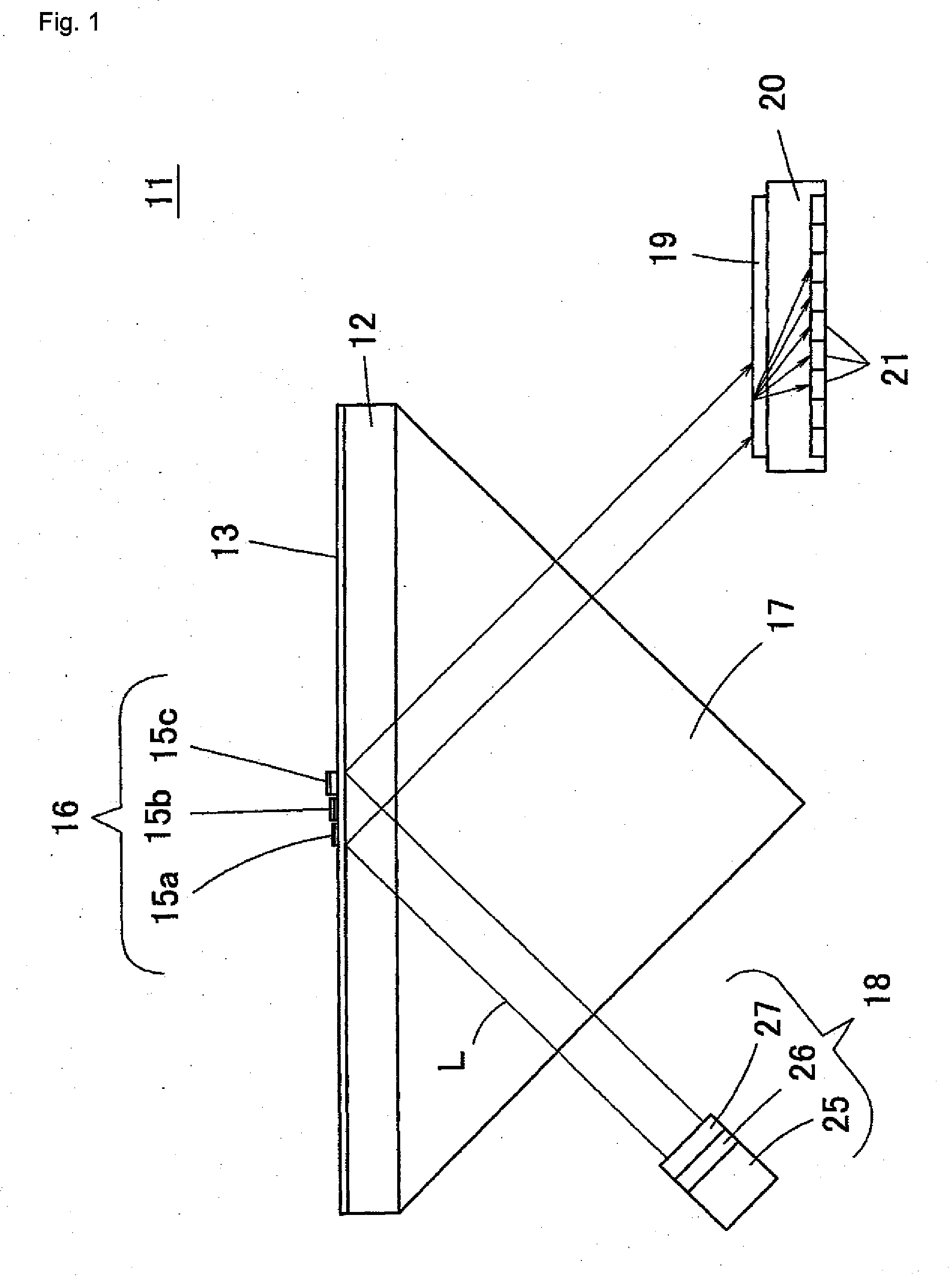
[0097]FIG. 1 is a schematic view illustrating a surface plasmon resonance sensor 11 according to the first example. The surface plasmon resonance sensor 11 according to the first example is a bulk-type surface plasmon resonance sensor including a prism 17 and employs so-called Kretschmanm placement.

[0098]The surface plasmon resonance sensor 11 includes a transparent substrate 12 made of a plastic such as PMMA, polycarbonate (PC) or polystyrene (PS) or a glass, and a metal layer 13 (metal thin film) formed on the entire surface of the transparent substrate 12. The transparent substrate 12 has a refractive index equal to that of the prism 17. The metal layer 13 is made of Au, Ag, Cu and the like formed on the upper surface of the transparent substrate 12 by vacuum deposition or sputtering.

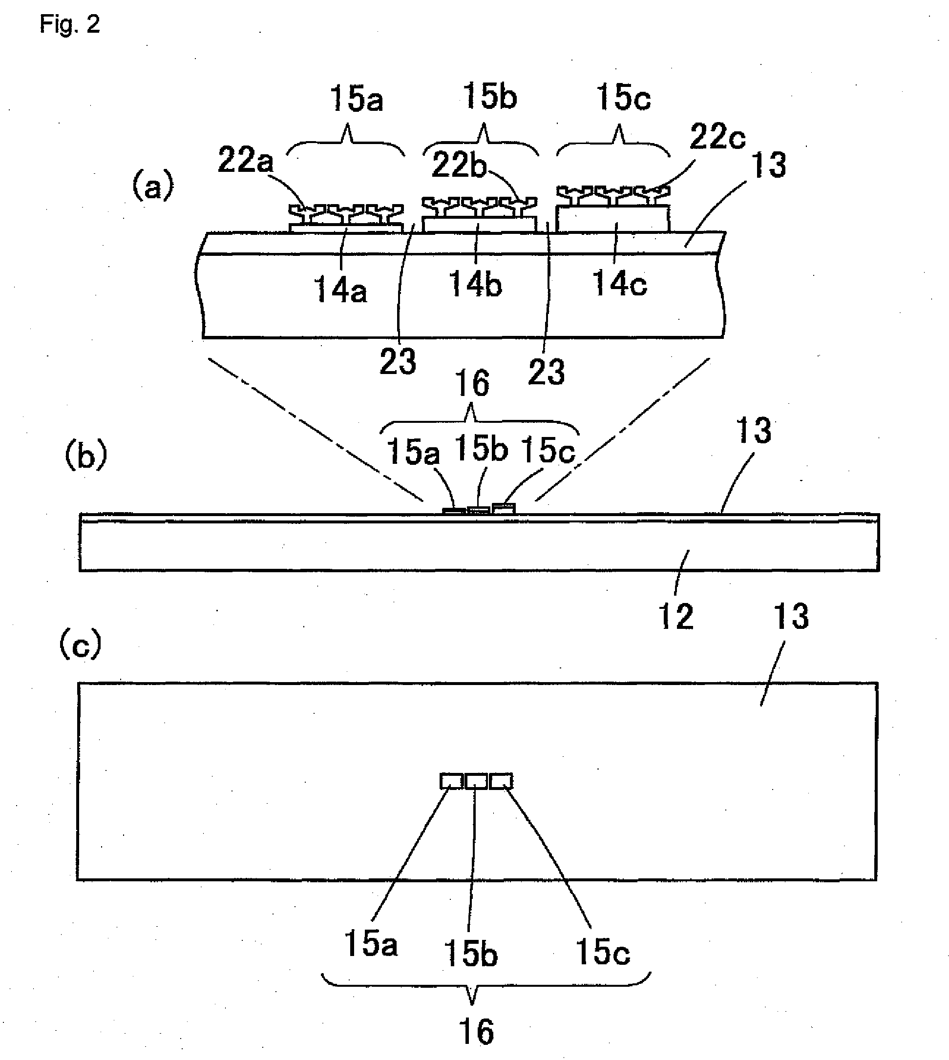
[0099]On the upper surface of the metal layer 13, there is formed a sample detection portion 16 constituted by a plurality of determination areas 15a, 15b, 15c. FIG. 2(a) is an enlarged view of the s...

second example

[0134]FIG. 13(a) is a schematic view illustrating a surface plasmon resonance sensor 31 according to a second example of the present invention, and FIG. 13(b) is a view illustrating a sample detection portion 16 therein, in an enlarged manner. In the first example, the metal layer 13 is formed in the areas outside of the determination areas 15a, 15b and 15c, but, in the surface plasmon resonance sensor 31 according to the second example, a metal layer 13 is not provided in the areas outside of determination areas 15a, 15b and 15c and is not exposed through the dielectric layers 14a, 14b and 14c. Accordingly, a transparent substrate 12 is exposed at the areas outside of the determination areas 15a, 15b and 15c, which enables applying hydrophilic processing or hydrophobic processing to the areas other than the determination areas 15a, 15b and 15c. This can prevent antigens from adhering to the areas other than the determination areas 15a, 15b and 15c, which can reduce signal noises du...

third example

[0136]FIG. 15 is a front view illustrating a surface plasmon resonance sensor 41 according to a third example of the present invention. FIG. 16(a) is an enlarged view of sample detection portions 16 in the surface plasmon resonance sensor 41. FIGS. 16(b) and (c) are a side view and a plan view of the sample detection portions 16 formed on the upper surface of a metal layer 13. In the surface plasmon resonance sensor 41 according to the third example, the sample detection portions 16 constituted by a plurality of determination areas 15a, 15b and 15c are arranged longitudinally and laterally (in the illustrated example, three sample detection portions are arranged in the longitudinal direction and four sample detection portions are arranged in the widthwise direction). Further, FIG. 17 is a plan view illustrating an array of light receiving devices 20, illustrating a plurality of light receiving devices 20 arranged longitudinally and laterally such that they correspond to the respecti...


PUM

PropertyMeasurementUnit
thicknessesaaaaaaaaaa
thicknessaaaaaaaaaa

Abstract

A metal layer 13 made of Au or the like is formed on the upper surface of a transparent substrate 12. Dielectric layers 14a, 14b and 14c with different thicknesses are formed on the upper surface of the metal layer 13 (any one of the dielectric layers can have a thickness of 0) to form respective determination areas 15a, 15b and 15c. Further, different types of antibodies 22a, 22b and 22c are fixed on the upper surfaces of the respective dielectric layers 14a, 14b and 14c. Then, light is directed to the determination areas 15a, 15b and 15c, then signals of light reflected by the determination areas 15a, 15b and 15c are received, the light is dispersed, and analyses are performed on signals resulted from the light dispersion to detect the conditions of the surfaces of the respective determination areas, at the same time.

Description

TECHNICAL FIELD[0001]The present invention relates to a surface plasmon resonance sensor chip and a surface plasmon resonance sensor. More specifically, the present invention relates to a surface plasmon resonance sensor which disperses the light of signals from a sample detection portion having a plurality of dielectric layers with different thicknesses for detecting the conditions of the surfaces of respective determination areas in the sample detection portion, a surface plasmon resonance sensor chip for use in the surface plasmon resonance sensor, and a medical inspection apparatus and a chemical-material inspection apparatus which employ the surface plasmon resonance sensor.BACKGROUND ART[0002]In recent years, diagnoses of health and constitutional predisposition of individual persons and foreseeing of illnesses have been increasingly enabled by inspections of genes and proteins of individual persons. As apparatuses for use therewith, there have been suggested various types of ...

Claims


Application Information

Patent Timeline
Patent Type & Authority Applications(United States)
IPC IPC(8): G01N21/55G01N21/27B29C59/02B44C1/22G01N21/41
CPCG01J3/02G01N21/553G01J3/0294G01J3/0256
Inventor MATSUSHITA, TOMOHIKOYAMASHITA, HIDEYUKINISHIKAWA, TAKEOMORIYAMA, MEGUMIHASUI, RYOSUKEAOYAMA, SHIGERU
Owner ORMON CORP
Why Eureka
Try Eureka