
Semiconductor Device and Wireless Tag Using the Same

a technology of semiconductor devices and wireless tags, applied in emergency protective arrangements, instruments, and emergency protection arrangements for limiting excess voltage/current, etc., can solve problems such as communication errors between r/w and wireless tags, noise input to signals, and large influence of antennas on transmitting and receiving signals

Inactive Publication Date: 2010-03-25
SEMICON ENERGY LAB CO LTD
View PDF18 Cites 32 Cited by
  • Summary
  • Abstract
  • Description
  • Claims
  • Application Information

AI Technical Summary

Benefits of technology

[0020]An overvoltage protection circuit included in an embodiment of the present invention receives a carrier wave or an amplitude modulation wave, and in the case where a generated voltage is close to an operation start voltage of the overvoltage protection circuit, after the overvoltage protection circuit starts operating once, a maximum value of the generated voltage is held by a memory circuit, whereby the overvoltage protection circuit is controlled in accordance with the held voltage. Therefore, the voltage at which the overvoltage protection circuit starts operating and the voltage at which the overvoltage protection circuit stops operating are different from each other. Thus, hysteresis occurs between the timing when the overvoltage protection circuit starts operating and the timing when the overvoltage protection circuit stops operating.
[0021]With such a structure, the overvoltage protection circuit operates such that the overvoltage protection circuit does not react sensitively to slight amplitude of received electric power of the carrier wave or the amplitude modulation wave and is stabilized; therefore, a modulation signal or demodulation signal is hardly affected by noise. Thus, in a wireless communication system using a R / W outputting high electric power, an internal circuit of a wireless tag is favorably protected from generation of an excessive voltage, and normal wireless communication can be stably performed without the electric power being changed due to modulation of the amplitude modulation wave.

Problems solved by technology

As described above, in transmitting and receiving an amplitude modulation wave whose modulation factor is small, noise generated in the periphery of an antenna greatly affects accuracy of transmitting and receiving signals.
As a result, noise is input to the signal.
Such noise causes a communication error between the R / W and the wireless tag.

Method used


Image

  • Semiconductor Device and Wireless Tag Using the Same
  • Semiconductor Device and Wireless Tag Using the Same
  • Semiconductor Device and Wireless Tag Using the Same

Examples


embodiment 1

[0037]Embodiment 1 of the present invention will be described with reference to FIG. 1.

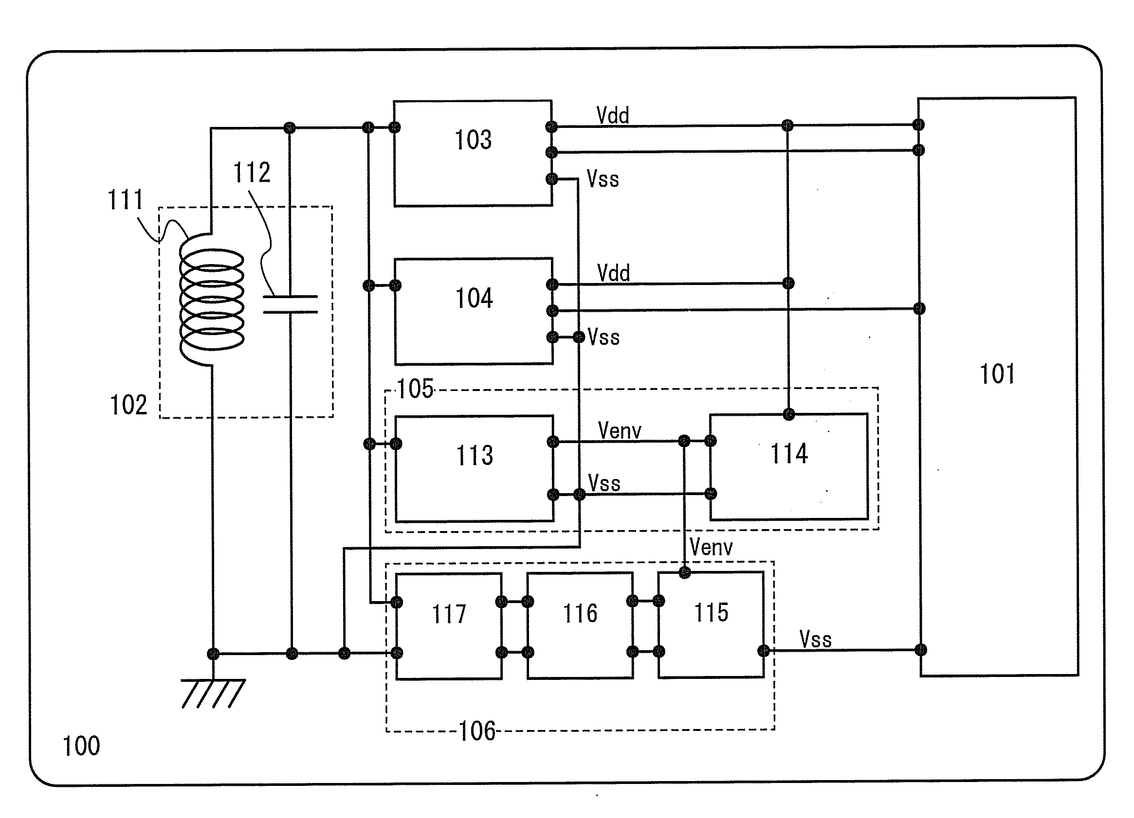
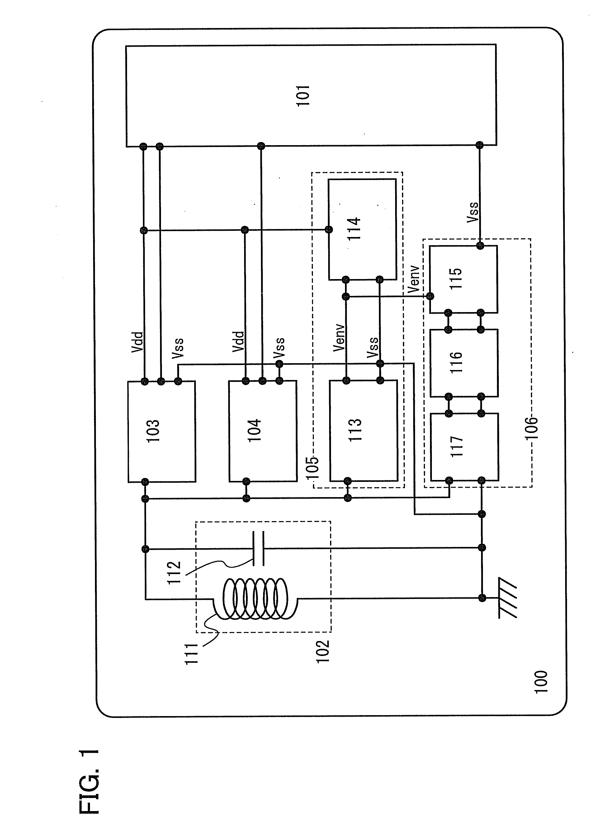
[0038]FIG. 1 is a block diagram of a wireless tag according to an embodiment of the present invention, and a wireless tag 100 includes: a logic circuit 101 for performing functional processing such as generating a response signal based on received data; an antenna circuit 102 for transmitting and receiving signals to / from a R / W; a demodulation circuit 103 for demodulating an amplitude modulation wave which is received by the antenna circuit 102 and extracting a pulse signal; a modulation circuit 104 for modulating the response signal which is output from the logic circuit 101 and converting the modulated signal into a signal which is transmitted to the R / W; a power supply circuit 105 for generating a DC voltage from a carrier wave or the amplitude modulation wave which is received by the antenna circuit 102; and an overvoltage protection circuit 106 according to an embodiment of the present invent...

embodiment 2

[0071]In this embodiment, one example of a method for manufacturing the semiconductor device described in the above embodiment is described.

[0072]First, a separation layer 1202 is formed over one surface of a substrate 1201. Then, an insulating film 1203 serving as a base and a semiconductor film 1204 (for example, a film containing amorphous silicon) are formed (see FIG. 12A). The separation layer 1202, the insulating film 1203, and the semiconductor film 1204 can be formed consecutively. By forming consecutively, they are not exposed to the air so that impurities can be prevented from being contained therein.

[0073]As the substrate 1201, a glass substrate, a quartz substrate, a metal substrate, a stainless steel substrate, a plastic substrate that can withstand the treatment temperature of the process described here, or the like can be used. When such a substrate is used, area and shape thereof are not restricted so much; therefore, by using a rectangular substrate with at least on...

embodiment 3

[0106]In this embodiment, a method for manufacturing a semiconductor device with higher reliability and high yield is described with reference to FIGS. 9A to 9D. In this embodiment, a CMOS (complementary metal oxide semiconductor) is described as an example of the semiconductor device.

[0107]Transistors 902 and 903, a capacitor 904, and an insulating layer 905 are provided over a formation substrate 900 with a separation layer 901 interposed therebetween, and a semiconductor integrated circuit 910 is formed (see FIG. 9A).

[0108]The transistors 902 and 903 are thin film transistors, and each include source and drain regions, a low-concentration impurity region, a channel formation region, a gate insulating layer, a gate electrode, and a source electrode or a drain electrode. The source and drain regions are in contact with wirings serving as source and drain electrodes, respectively, and electrically connected thereto.

[0109]The transistor 902 is an n-channel transistor, and includes an...


PUM


Abstract

In a wireless tag with which a wireless communication system whose electric power of a carrier wave from a R / W is high, an overvoltage protection circuit is provided to prevent from generating excessive electric power in the wireless tag when the wireless tag receives excessive electric power. However, as noise is generated by operation of the overvoltage protection circuit, an error of reception occurs in receiving a signal whose modulation factor is small. To solve the problem, the maximum value of generated voltage in the wireless tag is held in a memory circuit after the overvoltage protection circuit operates, then the overvoltage protection circuit is controlled in accordance with the maximum value of generated voltage. The voltages at which the overvoltage protection circuit starts and stops operating are different from each other, and hysteresis occurs between the timing when the overvoltage protection circuit starts and stops operating.

Description

TECHNICAL FIELD[0001]The present invention relates to a wireless tag which transmits and receives data using wireless communication. In particular, the present invention relates to a structure of an overvoltage protection circuit which prevents breakdown of a wireless communication circuit, or prevents deterioration or breakdown of an element included in the circuit in the case where a large amount of electric power is received in wireless communication.BACKGROUND ART[0002]In recent years, an individual identification technology using wireless communication (hereinafter referred to as a wireless communication system) has attracted attention. In particular, as a data carrier which transmits and receives data by wireless communication, an individual identification technology with a wireless tag (hereinafter collectively referred to as a “wireless tag” regardless of the shape such as a card shape or a chip shape) utilizing an RFID (radio frequency identification) technology has attract...

Claims


Application Information

Patent Timeline
Patent Type & Authority Applications(United States)
IPC IPC(8): G06K19/07H02H3/20
CPCG06K19/0707G06K19/0712H01L27/0251G06K19/07749G06K19/0715
Inventor NISHIJIMA, TATSUJI
Owner SEMICON ENERGY LAB CO LTD
Learn More