

Lateral graphene heat spreaders for electronic and optoelectronic devices and circuits
- Summary
- Abstract
- Description
- Claims
- Application Information
AI Technical Summary
Benefits of technology
Problems solved by technology
Method used
Image

Examples
first embodiment
[0057]FIG. 8 illustrates a A layer of buffer material 800 is placed on a device substrate 802. In one embodiment, the buffer material layer 800 is provided to facilitate graphene growth, for example, by epitaxial growth, CVD, and the like, or placement of the mechanically exfoliated graphene on top of the buffer material layer 800.
[0058]Alternatively, when graphene is produced by heat treatment of SiC, the substrate 802 and the buffer material layer 800 may be replaced by a SiC wafer. In one embodiment, the buffer material 800 includes a lattice structure similar to that of graphene (namely, hexagonal), thus allowing growth or incorporation of graphene on the buffer material layer 800. Buffer materials with high thermal conductivity are preferable. Suitable materials for the buffer material layer 800 are described below, and, as discussed below, the specific buffer material 800 may depend on the material of the substrate 802. The thickness of the buffer material layer 800 may vary ...
second embodiment
[0061]FIG. 9 illustrates a This embodiment is similar to other embodiments, except there is no buffer layer between a substrate 900 and a graphene layer 902. This embodiment may be employed when the substrate material and the graphene have matching lattice structures, or when graphene can be successfully grown directly on the substrate 900, thus making placement of the buffer layer redundant. The insulating layer 806 may include a synthetic polycrystalline diamond or other electrically insulating heat conducting materials. The incorporation of graphene with the room-temperature thermal conductivity of up to ˜5000 Wm−1K−1 significantly improves the lateral heat spreading.
third embodiment
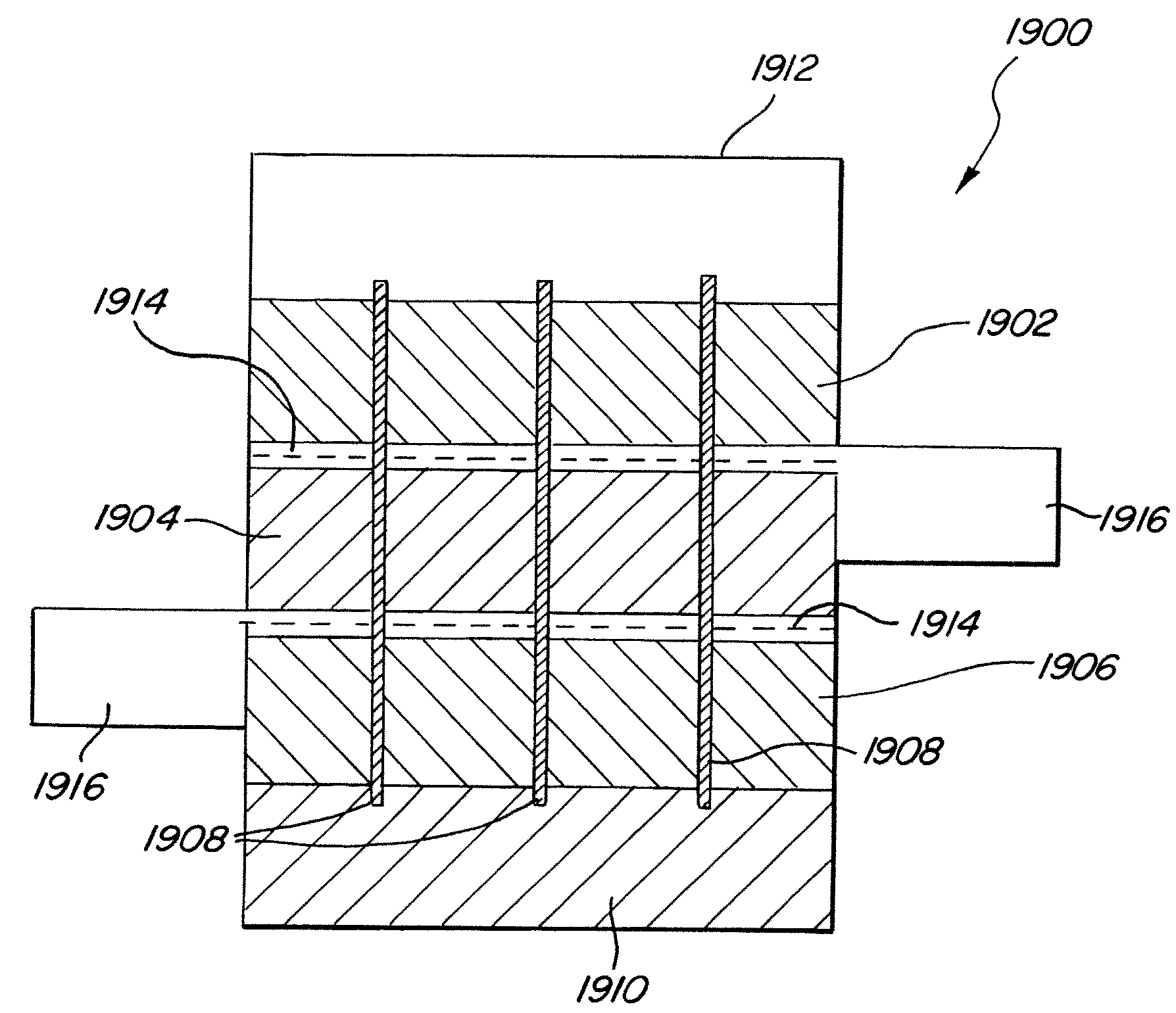
[0062]FIG. 10 illustrates a This embodiment is similar to the above-described embodiments, with a buffer 1002 disposed between at least a portion of substrate 1000 and at least a portion of one graphene layer 1004. In this embodiment, however, the substrate 1000 may be provided with a plurality of grooves 1006, into each of which a piece of thermally conductive material 1008, such as bulk graphite is disposed. The graphene layer(s) 1004 are formed on the substrate in a manner to contact the thermally conductive material 1008, which serve as heat sinks. The thermal conductivity of the material 1008 may have a very broad range of values. For example, a maximum achievable value is about 2000 Wm−1K−1 which is a single crystal plane thermal conductivity. This embodiment allows somewhat faster heat removal from the heat source where the material of the substrate has a thermal conductivity that is lower than that of thermally conductive material 1008, for example, Si (˜147 Wm−1K−1).
[0063]...
PUM
 Abstract
Description
Claims
Application Information