

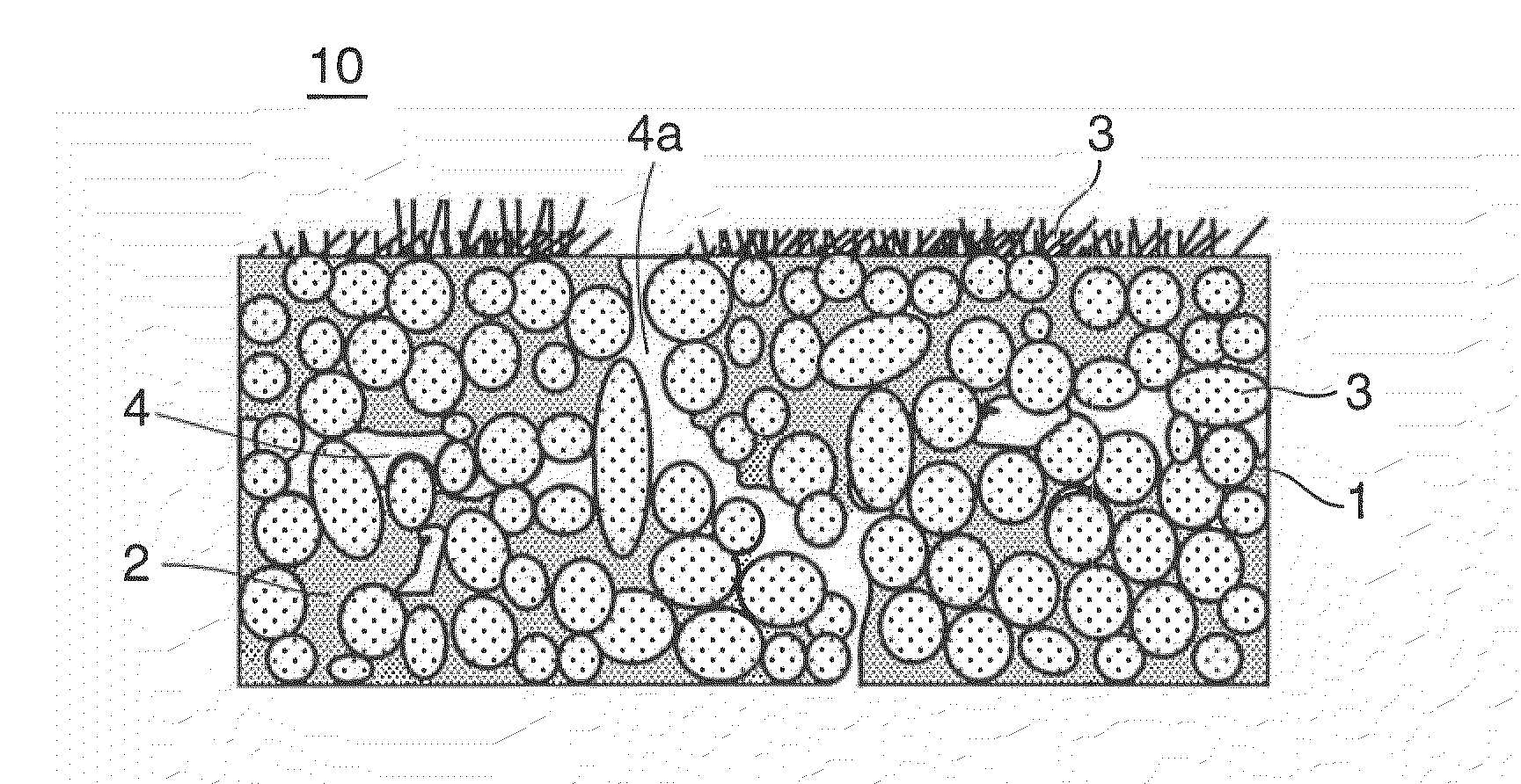
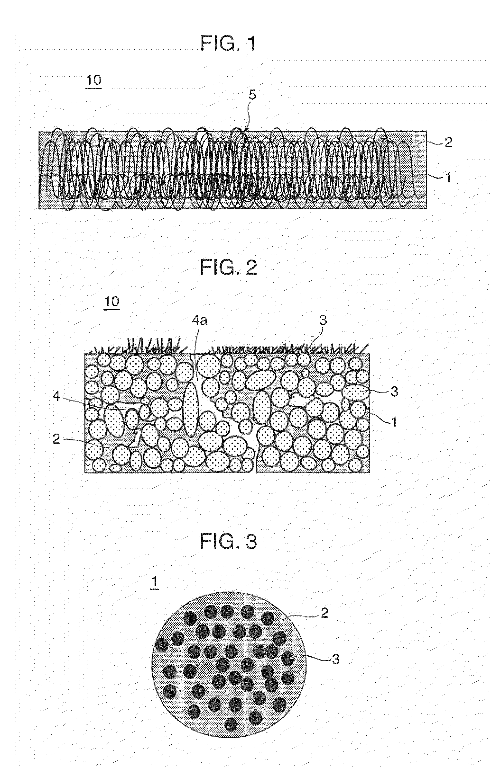
Polishing pad, and method for manufacturing polishing pad
a technology of polishing pad and polishing surface, which is applied in the direction of gear teeth, grinding devices, manufacturing apparatus of gear teeth, etc., can solve the problems of uneven polishing rate, uneven surface, and increased scratching or interfacial separation of polishing surface, etc., and achieve excellent flattening performance and resistance to scratching
- Summary
- Abstract
- Description
- Claims
- Application Information
AI Technical Summary
Benefits of technology
Problems solved by technology
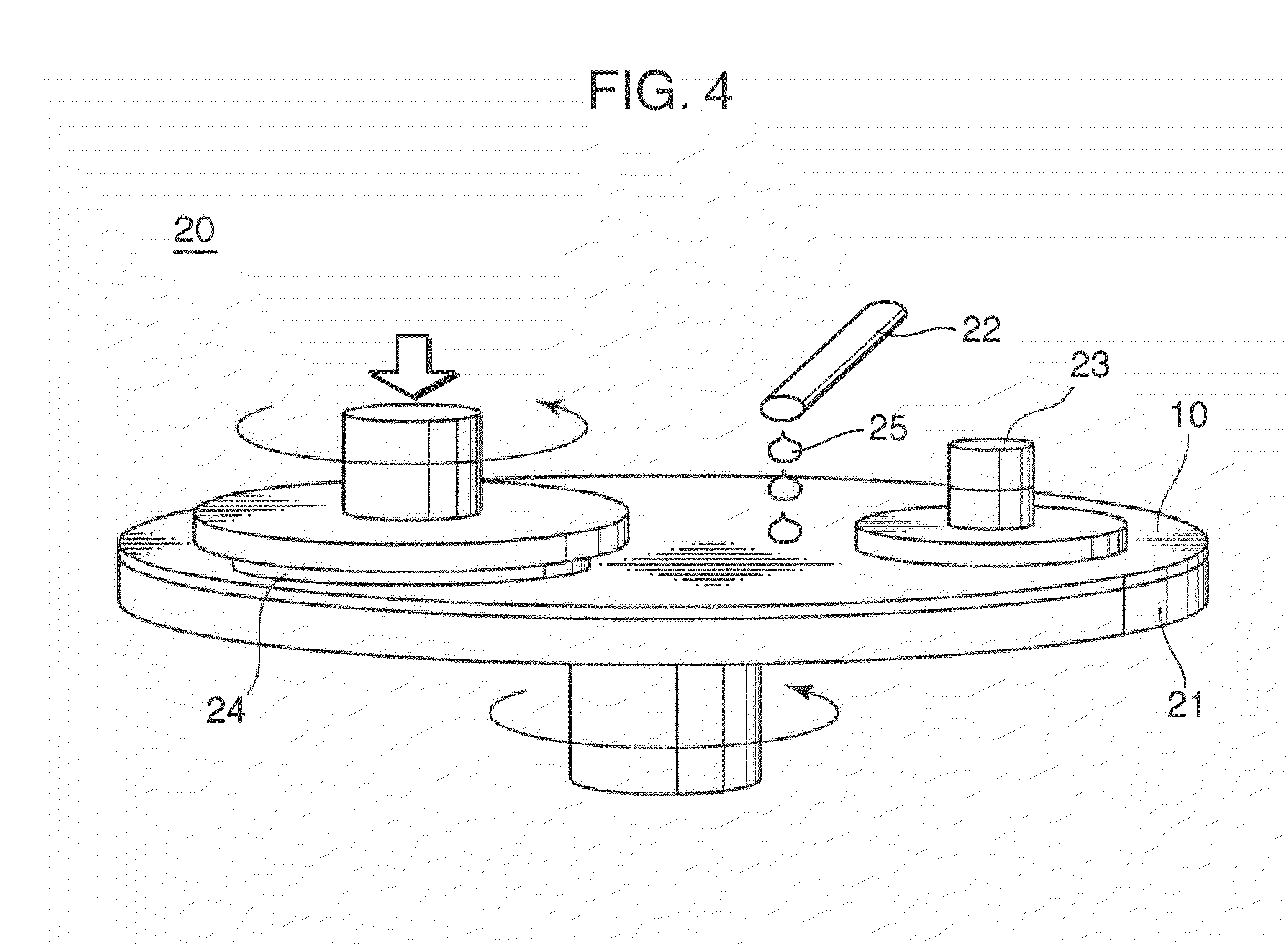
Method used
Image

Examples
working examples
Working Example 1
[0188]An islands-in-the-sea composite fiber was formed by discharging a water-soluble thermoplastic polyvinyl alcohol resin (hereinafter referred to as PVA resin) and isophthalic acid-modified polyethylene terephthalate with a degree of modification of 6 mol % (hereinafter referred to as modified PET; Tg of 77° C., water absorbency of 1 mass, nominal water content of 0.4 mass %) in a ratio of 20:80 (mass ratio) from a composite melt spinning nozzle. The composite melt spinning nozzle had 25 islands per fiber and a nozzle temperature of 260° C. The ejector pressure was adjusted to achieve a spinning rate of 4000 m / min, and long fibers with an average size of 2.0 dtex were caught in a net to obtain a spun-bond sheet (long fiber web) with a basis weight of 30 g / m2.
[0189]16 sheets of the spun-bond sheets thus obtained were cross-lapped to produce a lapped web with a total basis weight of 480 g / m2. The lapped web thus obtained was sprayed with an oil to prevent needle br...
working example 2
[0196]An islands-in-the-sea composite fiber was formed by discharging the PVA resin and the modified PET in a ratio of 25:75 (mass ratio) from a composite melt spinning nozzle. The composite melt spinning nozzle had 25 islands per fiber and a nozzle temperature of 260° C. The ejector pressure was adjusted to achieve a spinning rate of 4000 m / min, and long fibers with an average size of 2.0 dtex were caught in a net to obtain a spun-bond sheet (long fiber web) with a basis weight of 30 g / m2.
[0197]18 sheets of the spun-bond sheets thus obtained were cross-lapped to produce a lapped web with a total basis weight of 540 g / m2. The stacked web thus obtained was sprayed with an oil to prevent needle breakage. Then, the stacked web was entangled by needle punching at 1800 punches / cm2 using a No. 42 needle with one barb and a No. 42 needle with six barbs, which gave a web entangled sheet. The resulting web entangled sheet had a basis weight of 830 g / m2 and an interlayer separation strength o...
working example 3
[0203]An islands-in-the-sea composite fiber was formed by discharging the PVA resin and the modified PET in a ratio of 20:80 (mass ratio) from a composite melt spinning nozzle. The composite melt spinning nozzle had 25 islands per fiber and a nozzle temperature of 260° C. The ejector pressure was adjusted to achieve a spinning rate of 4000 m / min, and long fibers with an average size of 2.0 dtex were caught in a net to obtain a spun-bond sheet (long fiber web) with a basis weight of 30 g / m2.
[0204]18 sheets of the spun-bond sheets thus obtained were cross-lapped to produce a lapped web with a total basis weight of 540 g / m2. The lapped web thus obtained was sprayed with an oil to prevent needle breakage. Then, the lapped web was entangled by needle punching at 2000 punches / cm2 using a No. 42 needle with one barb and a No. 42 needle with six barbs, which gave a web entangled sheet. The resulting web entangled sheet had a basis weight of 870 g / m2 and an interlayer separation strength of ...
PUM
| Property | Measurement | Unit |
|---|---|---|
| Temperature | aaaaa | aaaaa |
| Temperature | aaaaa | aaaaa |
| Fraction | aaaaa | aaaaa |
Abstract
Description
Claims
Application Information