RF amplification device

a technology of amplification device and amplification device, which is applied in the direction of low noise amplifier, gated amplifier, amplifier with field-effect device, etc., can solve the problems of restricted frequency band and large circuit size, and achieve the effect of avoiding the increase of the height of the rf module and avoiding the increase of the occupied area

Inactive Publication Date: 2010-04-15
RENESAS ELECTRONICS CORP
View PDF11 Cites 24 Cited by
  • Summary
  • Abstract
  • Description
  • Claims
  • Application Information

AI Technical Summary

Benefits of technology

[0028]The following explains briefly the effect acquired by the typical one of the inventions disclosed by the present application.
[0029]That is, according to the present invention, in realizing a high-performance load in an RF amplification device, it is possible to avoid increase of a module height of an RF module, and at the same time, to avoid increase of an occupied area of a load circuit of a high-frequency amplifier which is formed over a semiconductor chip or a multilayer wiring circuit substrate.

Problems solved by technology

The traditional technique which uses these component parts results in a restricted frequency band and a large circuit size.

Method used


Image

  • RF amplification device
  • RF amplification device
  • RF amplification device

Examples


Embodiment Construction

1. >

[0061]First, an outline is explained on a typical embodiment of the invention disclosed in the present application. A numerical symbol in parentheses referring to a component of the drawing in the outline explanation about the typical embodiment only illustrates what is included in the concept of the component to which the numerical symbol is attached.

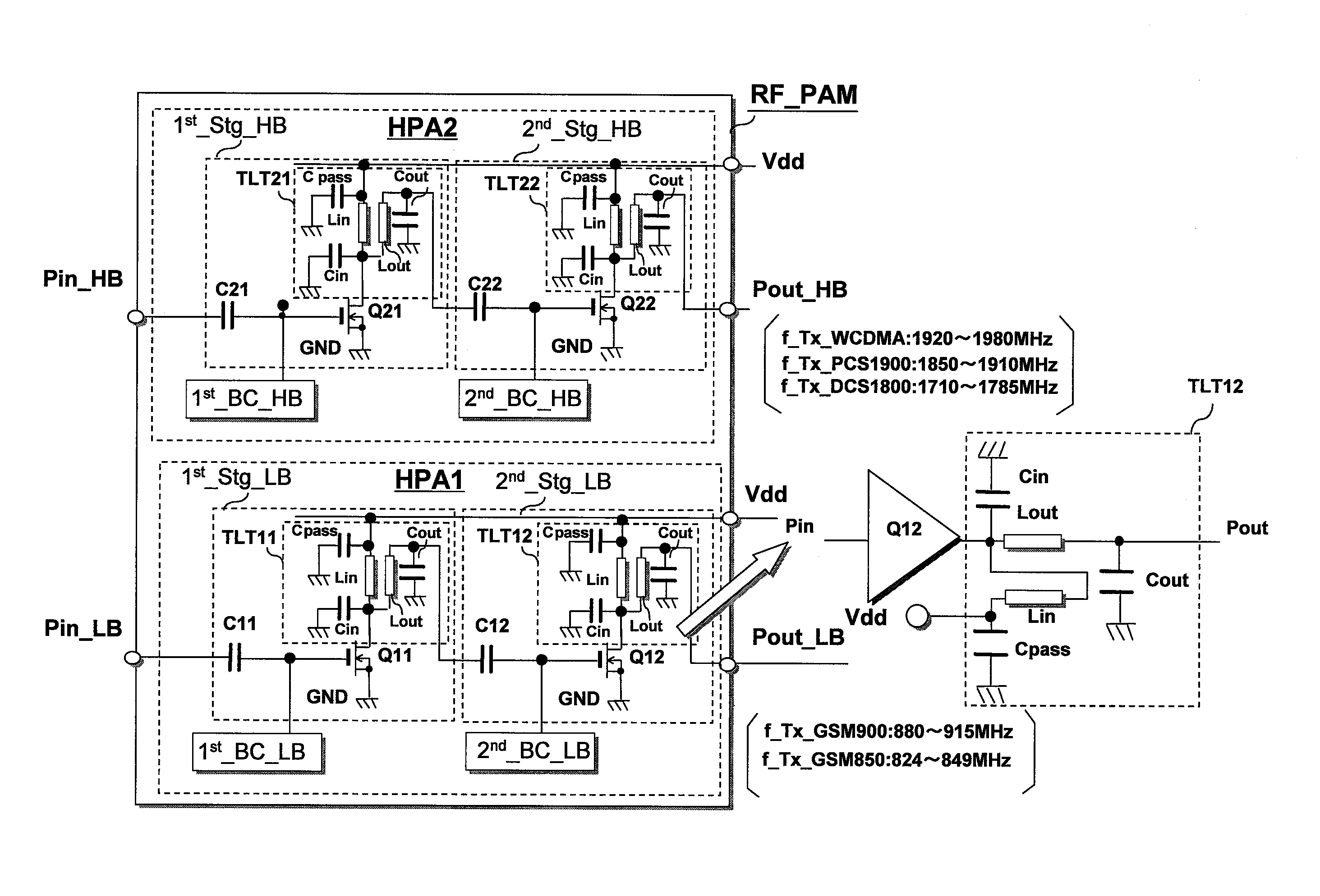
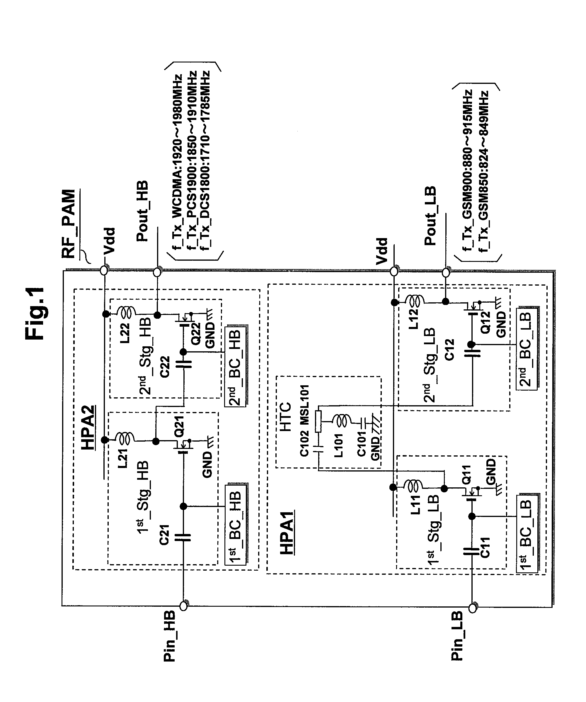
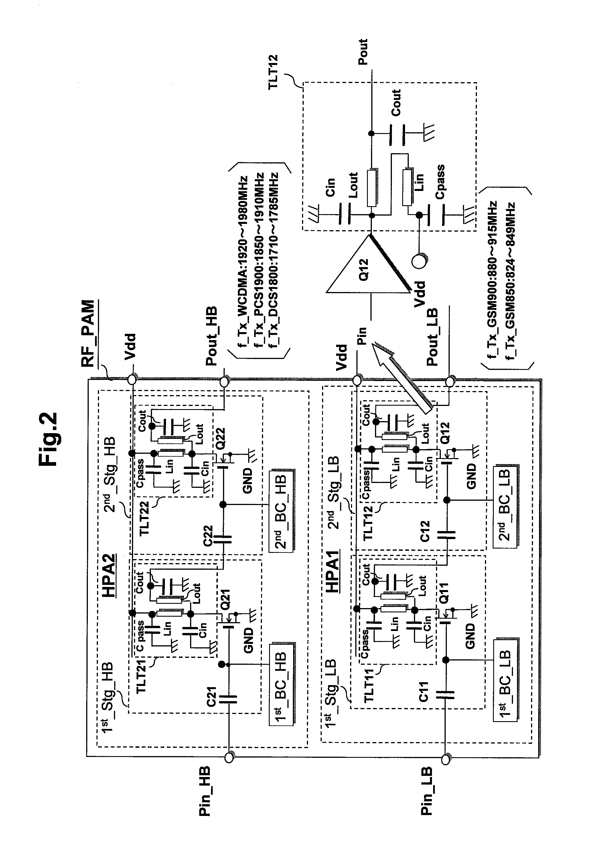
[0062](1) An RF amplification device according to a typical embodiment of the present invention comprises an amplification element (Q12) which amplifies a radio frequency input signal in wireless radio communication, and a transmission line transformer (TLT12) coupled to at least one electrode of an input electrode and an output electrode of the amplification element concerned. The transmission line transformer comprises a main line (Lout) arranged between an input and an output and a sub line (Lin) arranged between an AC ground point and one of the input and the output, and coupled to the main line. One of the input and the output...


PUM


Abstract

An RF amplification device has amplification elements which amplify a radio frequency input signal in wireless radio communication. Transmission line transformers are coupled to one of an input electrode and an output electrode of the amplification elements and have a main line Lout arranged between the input and the output, and a sub line Lin1 arranged between an AC ground point and one of the input and the output and coupled to the main line Lout. By applying an operating voltage different from the ground voltage level to the AC ground point, the operating voltage is supplied to the output electrodes of the amplification elements via the sub line from the AC ground point. In realizing a high-performance load circuit in an RF amplification device, it is possible to avoid increase of a module height of an RF module.

Description

TECHNICAL FIELD[0001]The present invention relates to an RF (radio frequency) amplification device, in particular, to technique which is useful for avoiding increase of a module height of an RF module, and at the same time, for avoiding increase of an occupied area of a load circuit of a high-frequency amplifier formed over a semiconductor chip or a multilayer wiring circuit substrate.BACKGROUND ART[0002]Plural communication modes exist in mobile communications represented by a mobile-phone. For example in Europe, in addition to GSM which has been in widespread use as the second generation wireless communication system, and EDGE which has enhanced a data transmission speed of GSM, there is W-CDMA of which the service has started in recent years as the third generation wireless communication system. In North America, in addition to DCS and PCS which are the second generation wireless communication systems, cdma1× has been in widespread use as the third generation wireless communicati...

Claims


Application Information

Patent Timeline
Patent Type & Authority Applications(United States)
IPC IPC(8): H03F3/16H03F1/00
CPCH03F1/0272H03F2203/7209H03F3/195H03F3/245H03F3/601H03F3/602H03F3/68H03F3/72H03F2200/108H03F2200/111H03F2200/18H03F2200/207H03F2200/255H03F2200/294H03F2200/318H03F2200/387H03F2200/391H03F2200/411H03F2200/423H03F2200/451H03F2200/456H03F2200/462H03F2200/465H03F2200/537H03F2200/541H03F2203/7206H03F1/565
Inventor OHNISHI, MASAMITANAKA, SATOSHITANAKA, RYOUICHI
Owner RENESAS ELECTRONICS CORP
Why Eureka
Try Eureka