

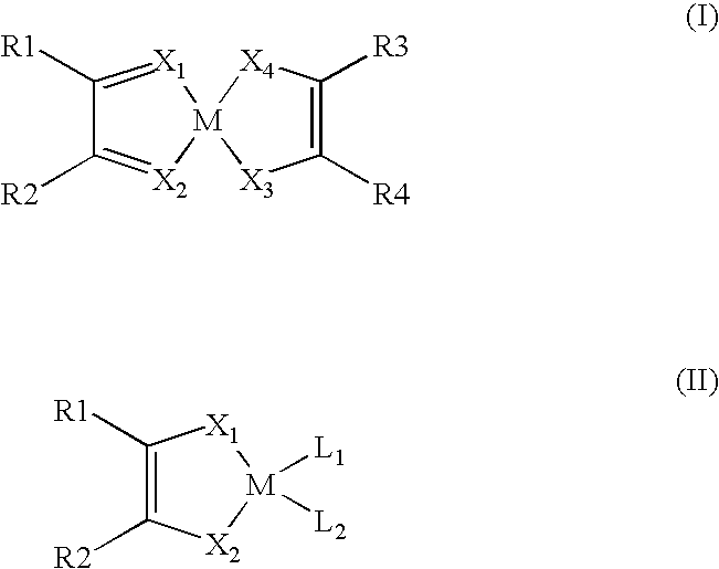
Square Planar Transition Metal Complexes and Organic Semiconductive Materials Using Them as Well as Electronic or Optoelectric Components
a technology of semiconductive materials and transition metal complexes, applied in the direction of non-metal conductors, conductors, organic semiconductor devices, etc., can solve the problems of affecting the function and stability of electronic components, affecting the properties of the doped layer and the corresponding electronic component, and often insufficient reduction potential of such released dopants
- Summary
- Abstract
- Description
- Claims
- Application Information
AI Technical Summary
Benefits of technology
Problems solved by technology
Method used
Image

Examples
examples of application
[0061]An extremely electron-poor transition metal complex compound is prepared in a very clean manner.
[0062]The proposed electron-poor transition metal complex compound is evaporated at the same time with the matrix material. According to the exemplary embodiment the matrix material is zinc phthalocyanine, spiro-TTB or a-NDP. The p-dopant and the matrix material can be evaporated in such a manner that the layer precipitated on the substrate in a vacuum evaporation system has a doping ratio of p-dopant to matrix material of 1:10.
[0063]The particular layer of the organic semiconductor material doped with the p-dopant is applied on an ITO layer (indium tin oxide) arranged on a glass substrate. After the application of the p-doped organic semiconductor layer a metal cathode is applied, for example, by vapor-depositing a suitable metal on it in order to produce an organic light-emitting diode. It is understood that the organic light-emitting diode can also have a so-called inverted layer...
specific example
[0064]
example
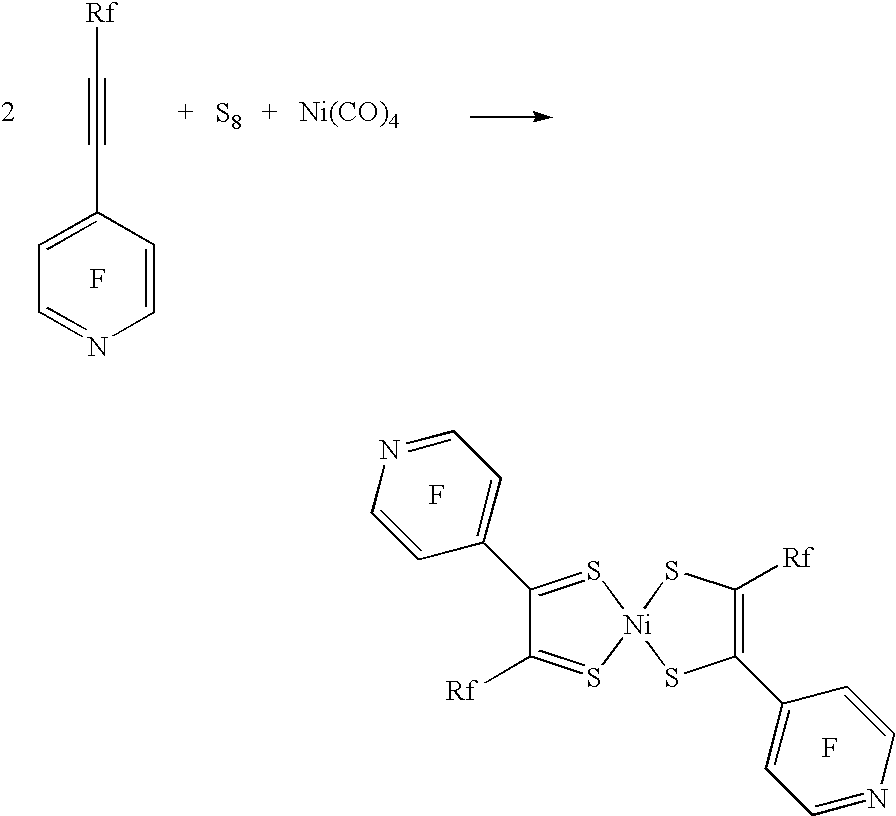
[0065]The nickel complex EX1 was synthesized according to the procedure below:
[0066]The compound (1) passed as Vapour (or gas) trough boiling sulfur to obtain compound (2), which is used as raw material, without further purification. Compound (2) was reacted with RANEY Nickel in toluene solution to obtain the final compound. This was purified by column chromatography (MPLC) on silica with hexane as eluent. The mass spectra analysis shows a very clear peak at m / z=574.
PUM
| Property | Measurement | Unit |
|---|---|---|
| thick | aaaaa | aaaaa |
| conductivity | aaaaa | aaaaa |
| conductivity | aaaaa | aaaaa |
Abstract
Description
Claims
Application Information