Film Thickness Measuring Method and Substrate Processing Apparatus

Inactive Publication Date: 2010-04-22
EBARA CORP
View PDF12 Cites 8 Cited by
  • Summary
  • Abstract
  • Description
  • Claims
  • Application Information

AI Technical Summary

Benefits of technology

[0020]By determining a thickness of an oxide film or a thin film by solely using a phase difference Δ among various optical parameters measurable by ellipsometry, e.g., of the single-wavelength type, according to the present invention, measurement of the oxide film or thin film can be carried out more simply in a shorter time as compared to a conventional common measuring method using ellipsometry, which calculates a thickness of a thin film from

Problems solved by technology

A film thickness measuring device using spectroscopic ellipsometry is thus complicated and large-sized, and incorporation of

Method used


Image

  • Film Thickness Measuring Method and Substrate Processing Apparatus
  • Film Thickness Measuring Method and Substrate Processing Apparatus
  • Film Thickness Measuring Method and Substrate Processing Apparatus

Examples


Example

[0028]Preferred embodiments of the present invention will now be described with reference to the drawings.

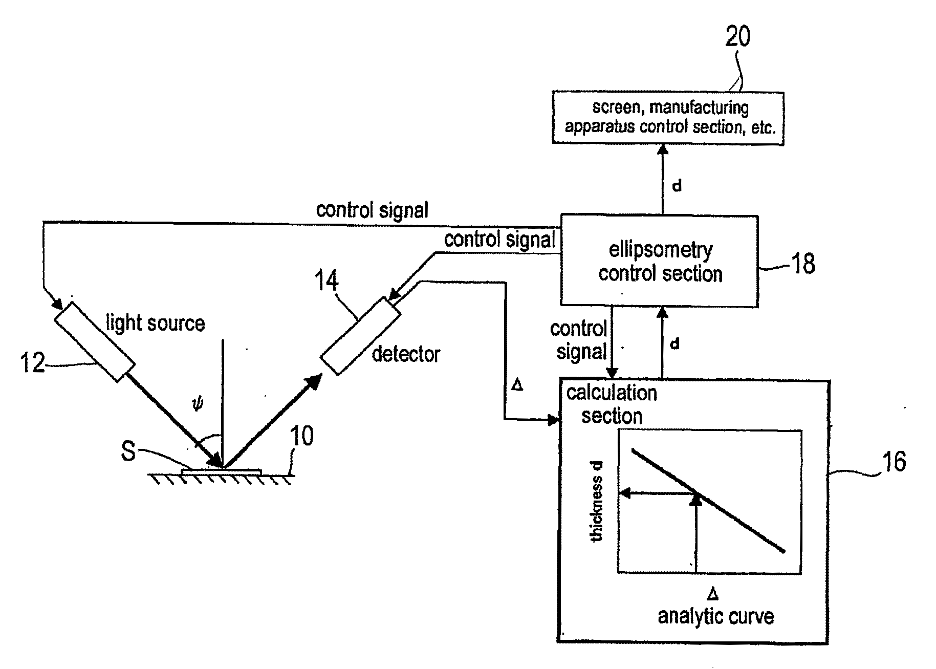
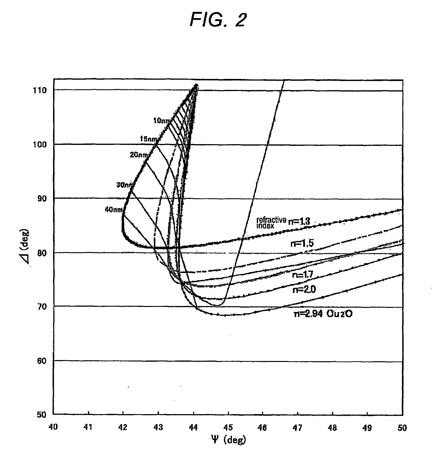
[0029]FIG. 1 shows a film thickness measuring device for measuring a thickness of, e.g., a native oxide film, formed in a surface of a substrate, by a film thickness measuring method according to the present invention. As shown in FIG. 1, the film thickness measuring device includes a sample stage 10 for placing thereon a sample S to be measured, e.g., a substrate, a light source 12 for emitting, e.g., He—Ne laser light (wavelength 632.8 nm) toward the sample S placed on the sample stage 10, and a detector 14 for receiving the laser light reflected from the sample S. The emitted laser light has been polarized into a linear polarized light by a polarizing plate provided in the light source 12 and is applied to a surface of the sample S. The linear polarized laser light, when reflected by the surface of the sample S, changes into an elliptical polarized light. The detector 14 meas...


PUM

PropertyMeasurementUnit
Thicknessaaaaaaaaaa
Thicknessaaaaaaaaaa

Abstract

A film thickness measuring method can carry out measurement of a thickness of an oxide film more simply in a shorter time. The film thickness measuring method includes determining a thickness of an oxide film or thin film of a metal or alloy by solely using a phase difference Δ, measured by ellipsometry, based on a predetermined relationship between the phase difference Δ and the thickness of the oxide film or thin film of the metal or alloy.

Description

TECHNICAL FIELD[0001]The present invention relates to a film thickness measuring method which is useful, for example, for measuring a thickness of an oxide film, formed in a surface of a metal film, prior to removing the oxide film in a semiconductor device manufacturing process. The present invention also relates to a substrate processing apparatus which is useful, for example, for forming embedded interconnects by filling an interconnect material into interconnect recesses, such as trenches and via holes, provided in a surface of a substrate such as a semiconductor wafer.BACKGROUND ART[0002]With the progress toward finer semiconductor devices, copper is becoming a common interconnect material these days. Further, various metal materials that have not been conventionally used for semiconductor devices, are now in practical use; for example, cobalt for a gate electrode and tantalum as a barrier metal. Hafnium is being studied for its use for a gate insulating film. These metals, in ...

Claims


Application Information

Patent Timeline
IPC IPC(8): G01B11/06C23C14/52B05C11/00B01J19/00G01J4/00C23G1/02
CPCG01B11/0641
Inventor SUSAKI, AKIRASHIMA, SHOHEIFUKUNAGA, YUKIOTATEISHI, HIDEKIMINE, JUNKO
Owner EBARA CORP
Why Eureka
Try Eureka