Assembling Stacked Substrates That Can Form 3-D Structures

a technology of stacked substrates and substrates, applied in semiconductor lasers, laboratory glassware, instruments, etc., can solve the problems of difficult replacement of discrete elements with switches formed, unfavorable systems, and inability to do, so as to reduce power dissipation, reduce leakage current, and maximize force

Inactive Publication Date: 2010-04-22
TRACKTHINGS
View PDF25 Cites 9 Cited by
  • Summary
  • Abstract
  • Description
  • Claims
  • Application Information

AI Technical Summary

Benefits of technology

[0007]Another embodiment is described which uses Coulomb forces to adjust the physical dimensions of antennas. Thus, antennas can be adjusted in the field to better match the carrier frequency. Several antennas: the Yagi, the patch, the bow-tie, the meanderline, and the dipole antenna can be adjusted to benefit from this adjustment. As more antennas can be placed on a substrate, additional flexibility occurs such as using an antenna at a given carrier frequency to transmit a signal while the second antenna can be used to receive the signal at a different carrier frequency. Conversely, the antennas can be used in a MIMO system to provide a multi-channel wireless communication where the antennas can be moved on the surface of a substrate to improve reception. One embodiment is the ability to rotate an antenna substrate 90° around the edge of a substrate. This allows antennas to be formed that exist in three orthogonal planes. Receiving and transmitting signals in three orthogonal dimensions improves reception if one of the signals fades in a given dimension. Many of these techniques are also applicable to inductor construction.
[0011]Another embodiment is increasing the number of Coulomb islands to decrease the required voltage that needs to be applied to the island. This helps in reducing the stress applied to the junctions and devices.
[0014]In another embodiment, a Faraday shield can be placed under the Coulomb island to isolate the Coulomb island from the remainder of the substrate. In addition, the potential of the Faraday shield can be altered to control the electric field leaving the substrate and thereby controlling the force being applied to a juxtaposed Coulomb island. Another embodiment is performing edge processing of a substrate. Vertical Coulomb islands and vertical Faraday shields can be formed. This inventive aspect allows Coulomb islands to be charged to attract two or more substrates along their edge.
[0015]In another embodiment, charge is induced in a metallic Coulomb island by an externally charged plate. The Coulomb island can have a probe opening to directly charge the island, and then this charged Coulomb island can be used to induce a charge on another Coulomb island. The probe opening can be mechanically probed using an external probe or a MEMS probe. In another embodiment, the gate of a non-volatile memory that is isolated is connected to a Coulomb island where the entire combined structure is surrounded by an insulator. The island is placed at the surface of the substrate to maximize the forces that can be generated between this island and another island located near the surface of a second substrate. Furthermore, several non-volatile devices can be connected to the island simultaneously where each device can be optimized to perform a special function.
[0016]In another embodiment, Coulomb forces are used to detach substrates from the system to decrease leakage current in that substrate to decrease power dissipation. An embodiment allows an inductor on a substrate to be levitated so that losses of the inductor are decreased. Another embodiment is wire bonding a substrate to power and DC supplies and using the Coulomb force to lift the substrate so that the substrate is levitated. Another embodiment is using the Coulomb forces between two substrates to cause one of the substrates to overhang a new substrate which does not have Coulomb islands. However, the substrate over hanging the new substrate can electrically connect to the new substrate to introduce a new circuit element into the new substrate.

Problems solved by technology

ASIC (Application Specific Integrated Circuit) and custom logic typically are unforgiving systems since an error in the logic may not allow for an easy recovery once the device has been fabricated.
There are situations where some systems that would desire the ability to be reconfigurable but currently are not able to do so.
It is difficult to replace these discrete elements with switches formed from active circuitry since the circuitry introduces loss and degrades the characteristics of the discrete elements.
An RF (Radio Frequency) switch is used to switch the antenna from the transmitter to the receiver and the switch itself unfortunately introduces a loss of about 0.5 db.
This is because it is difficult to replace metal with active components.
However, the switch introduces a loss and reduces the Q of the inductor; this is typically an undesirable effect.
These capacitors can behave nonlinearly and have a limited range of linear operation over a given voltage range.
Since the hardware is physically soldered and bound in place in the system, it is very difficult to replace them with hardware that has been optimized to operate at this newer frequency band.
The consequences are a loss in gain and not being able to achieve the ultimate performance with an optimum design.

Method used


Image

  • Assembling Stacked Substrates That Can Form 3-D Structures
  • Assembling Stacked Substrates That Can Form 3-D Structures
  • Assembling Stacked Substrates That Can Form 3-D Structures

Examples


Embodiment Construction

[0080]Several inventions are presented and are described in this specification. All the prior art that has been cited fail to show the inventive techniques including, but not limited to: a moving component that; 1) can be detached from its surroundings; 2) can contain Coulomb islands with opposing charges: 3) can freely move by using Coulomb forces formed by Coulomb charges, and; 4) can adjust the charge of the Coulomb islands in both magnitude and polarity.

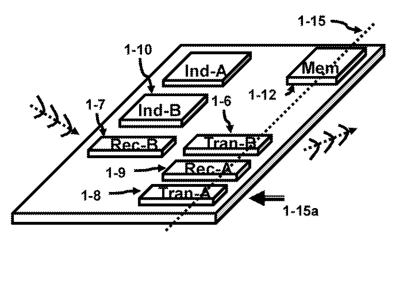
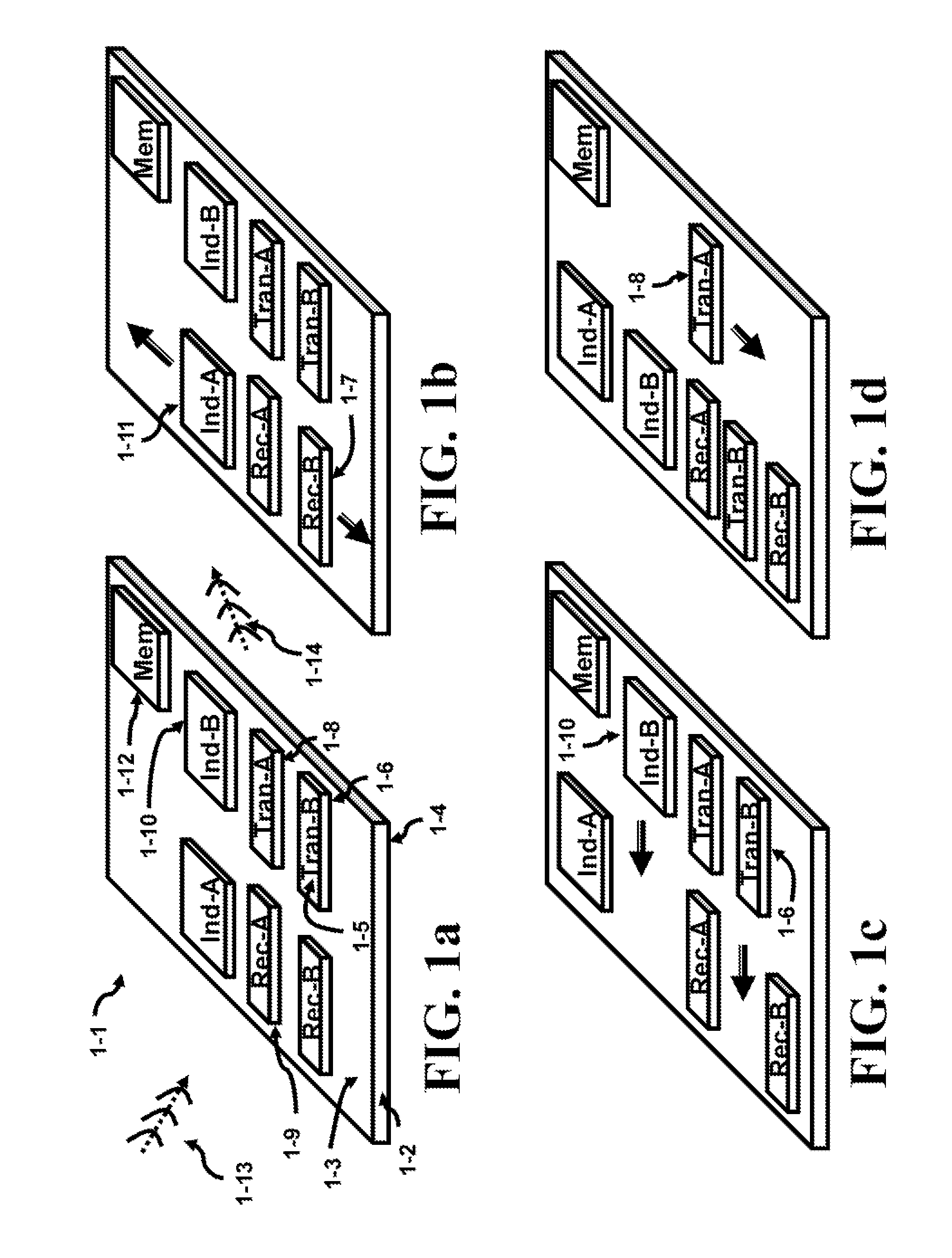
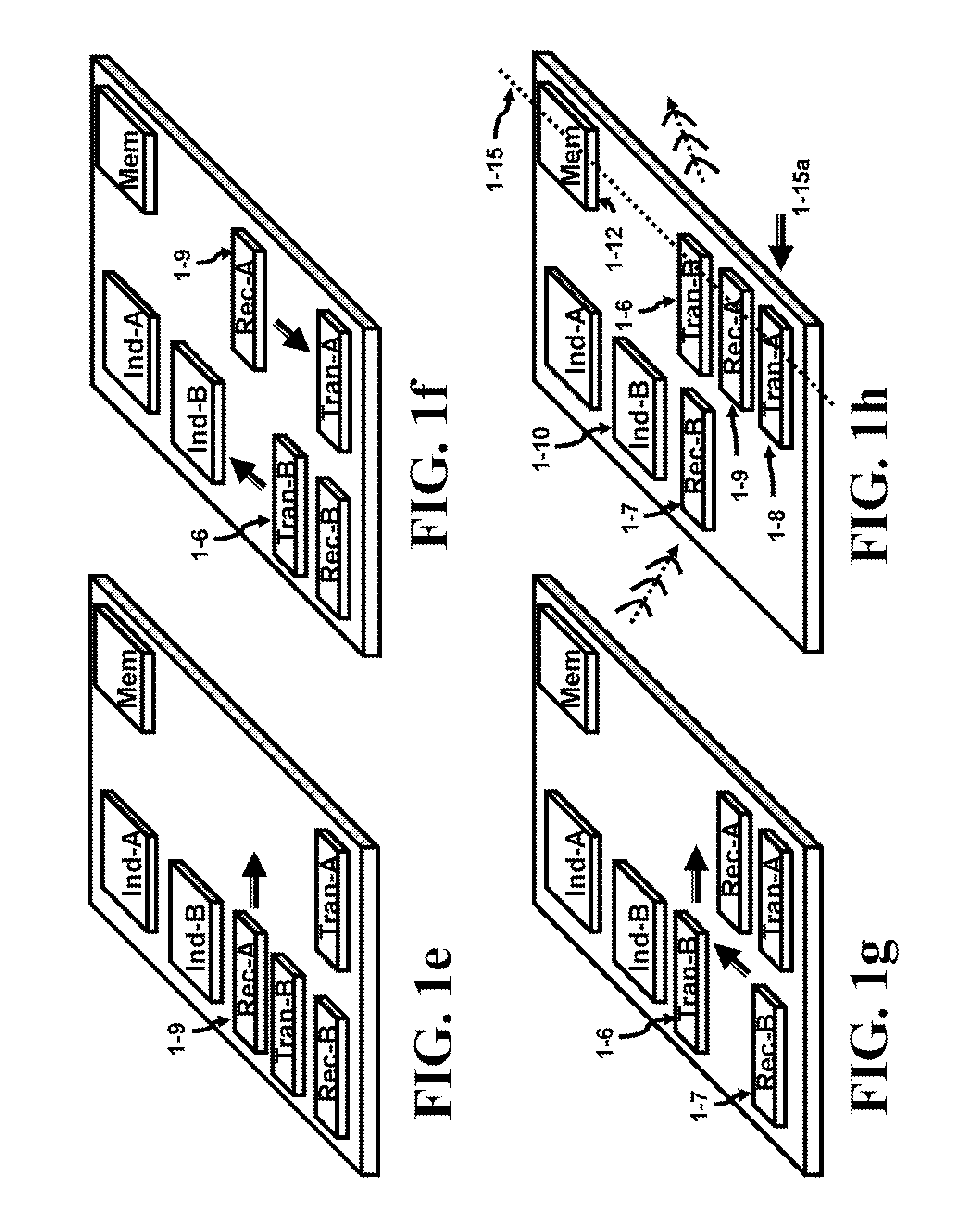
[0081]FIG. 1a shows a reconfigurable system 1-1 which uses Coulomb force to levitate and position the upper substrates on the top surface of the lower substrate. The lower substrate will be addressed as the mother substrate 1-2 while the upper ones (1-6 through 1-12) will be called the daughter substrates in several descriptions. The substrates can be a die, comprised of dice (chips), MCM (Multi Chip Modules), MEMS (Micro-Electro-Mechanical Systems), wafer bonded components or any of the previous combinations. For instance, a mem...


PUM

PropertyMeasurementUnit
timeaaaaaaaaaa
thicknessaaaaaaaaaa
displaced angleaaaaaaaaaa

Abstract

A system is described that can assemble substrates over one another to form a stacked substrate. The various layers of the stacked substrate can be separated from each other by using Coulomb forces. In addition, a beam substrate can be used to increase the separation. In addition, a first substrate can be flipped around and connected to the edge of a second substrate. The instructions for assembly and a FSM (Finite State Machine) can be included in the stacked substrate to pave the way for a self-constructing 3-D automaton. The beam substrate can be used to carry heat, fluids, electrical power or signals between the various layers of the stacked cells besides providing a mechanical support. A stacked substrate can be assembled into 3-D structures. These structures can have applications in antennas and RF circuits, for example.

Description

CROSS-REFERENCE TO RELATED APPLICATIONS[0001]This application is a divisional of U.S. patent application Ser. No. 11 / 953,002 filed Dec. 7, 2007, the disclosure of which is incorporated herein by reference. The ADS claims the benefit of co-filed applications that were invented by the same inventor as the present application, filed on Dec. 7, 2007, the disclosure of which is incorporated herein by reference.BACKGROUND OF THE INVENTION[0002]ASIC (Application Specific Integrated Circuit) and custom logic typically are unforgiving systems since an error in the logic may not allow for an easy recovery once the device has been fabricated. The re-design cycle time can be 3-4 months. An FPGA (Field Programmable Gate Array), however, is an on the fly reconfigurable Boolean logic system. The heart of Reconfigurable logic is the configurable logic block which is formed using Boolean logic and can be altered very easily since an input digital signal can modify the operation of the logic block wi...

Claims


Application Information

Patent Timeline
Patent Type & Authority Applications(United States)
IPC IPC(8): H05K1/14H05K3/36
CPCB01L3/502707B01L3/502715B01L2200/028B01L2200/10B01L2200/143B01L2300/0816B01L2300/0861G01P15/125G01P15/18H01L23/06H01L24/73H01L24/95H01L25/18H01L25/50H01L2224/13021H01L2224/32145H01L2224/48145H01L2224/48227H01L2224/83121H01L2224/95092H01L2224/95145H01L2924/01002H01L2924/01013H01L2924/01015H01L2924/01027H01L2924/01029H01L2924/01038H01L2924/01075H01L2924/01079H01L2924/01082H01L2924/10329H01L2924/14H01L2924/1433H01L2924/19041H01L2924/19042H01L2924/30105H01L2924/30107H01L2924/3011H01L2924/3025H01Q9/0407H01Q9/14H01Q9/16H01S5/183H01S5/4025H01L24/48H01L2924/01005H01L2924/01006H01L2924/01019H01L2924/01023H01L2924/01033H01L2224/32225H01L2224/73265H01L2924/15311H01L2924/10253B81C3/004B81C2203/051H01L2924/1461H01L2224/16235Y10T29/49126H01L2924/00H01L2224/451H01L2924/00014H01L2924/16195H01L2224/45099H01L2924/00012
Inventor GABARA, THADDEUS
Owner TRACKTHINGS
Why Eureka
Try Eureka