Flexible display substrates

a display substrate and flexible technology, applied in the field of thin film semiconductors, can solve the problems of poor uniformity, high manufacturing cost, poor electrical characteristics of amorphous silicon films, etc., and achieve the effect of enhancing low-charge carrier mobility and being more resistant to breakag

Inactive Publication Date: 2010-04-22
CORNING INC
View PDF16 Cites 4 Cited by
  • Summary
  • Abstract
  • Description
  • Claims
  • Application Information

AI Technical Summary

Benefits of technology

[0012]The processes of the present invention include steps of transferring a substantially uniform film with enhanced low-charge carrier mobility onto a polymer substrate to form a semiconductor structure that is flexible, lightweight, and more resistant to breakage. Processes in accordance with the present invention do not require the use of high temperatures or oxidized silicon layers.

Problems solved by technology

As a result, amorphous silicon films possess poor electrical characteristics and inherently poor stability.
Amorphous silicon film is suitable for producing transistors to switch individual pixels on and off, but is unable to handle logic and mixed signal functions needed for higher performance devices.
While this emerging technology is expected to eliminate the need for separate display drivers, required with TFTs made of amorphous silicon, and allow fabrication of drivers on poly-Si itself, and reduce the cost and size of display devices, poly-Si technology has been under development for several years and has yet to solve issues of poor uniformity and high cost of manufacture.
Since processes for obtaining an SCS film on a substrate require relatively high temperatures, they are not suitable for polymer substrates.
However, glass substrates result in significant weight of display devices due to the high density of glass employed therein.
Also, glass substrates are rigid and possess a low tolerance for bending stresses.
Moreover, glass is fragile and if dropped, TFTs made with glass substrates have a high risk of breakage.
These technologies employ either amorphous silicon or poly-Si film transferred to a polymer substrate and are subject to the aforementioned drawbacks.

Method used


Image

  • Flexible display substrates
  • Flexible display substrates
  • Flexible display substrates

Examples


example 1

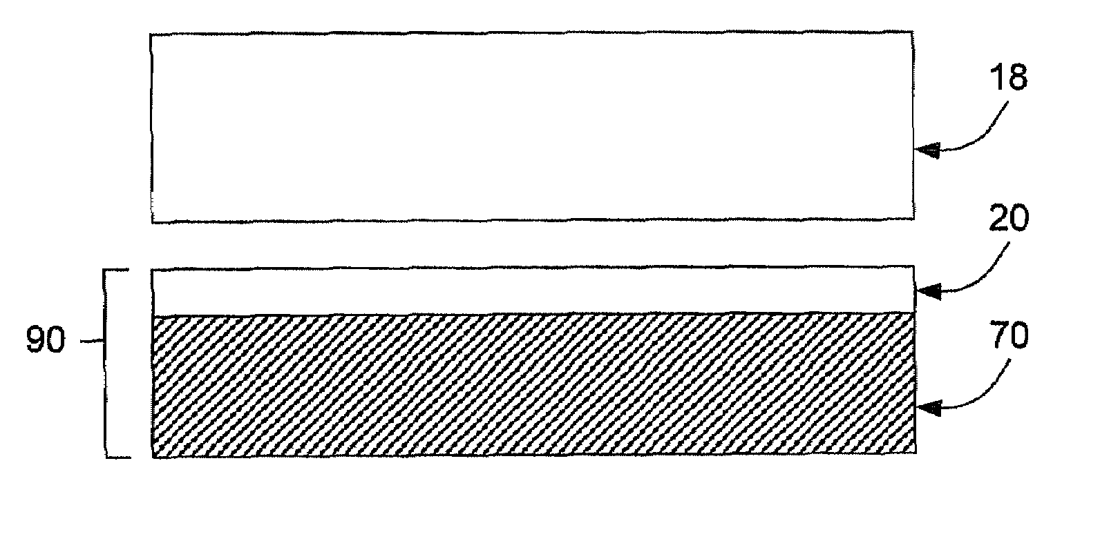
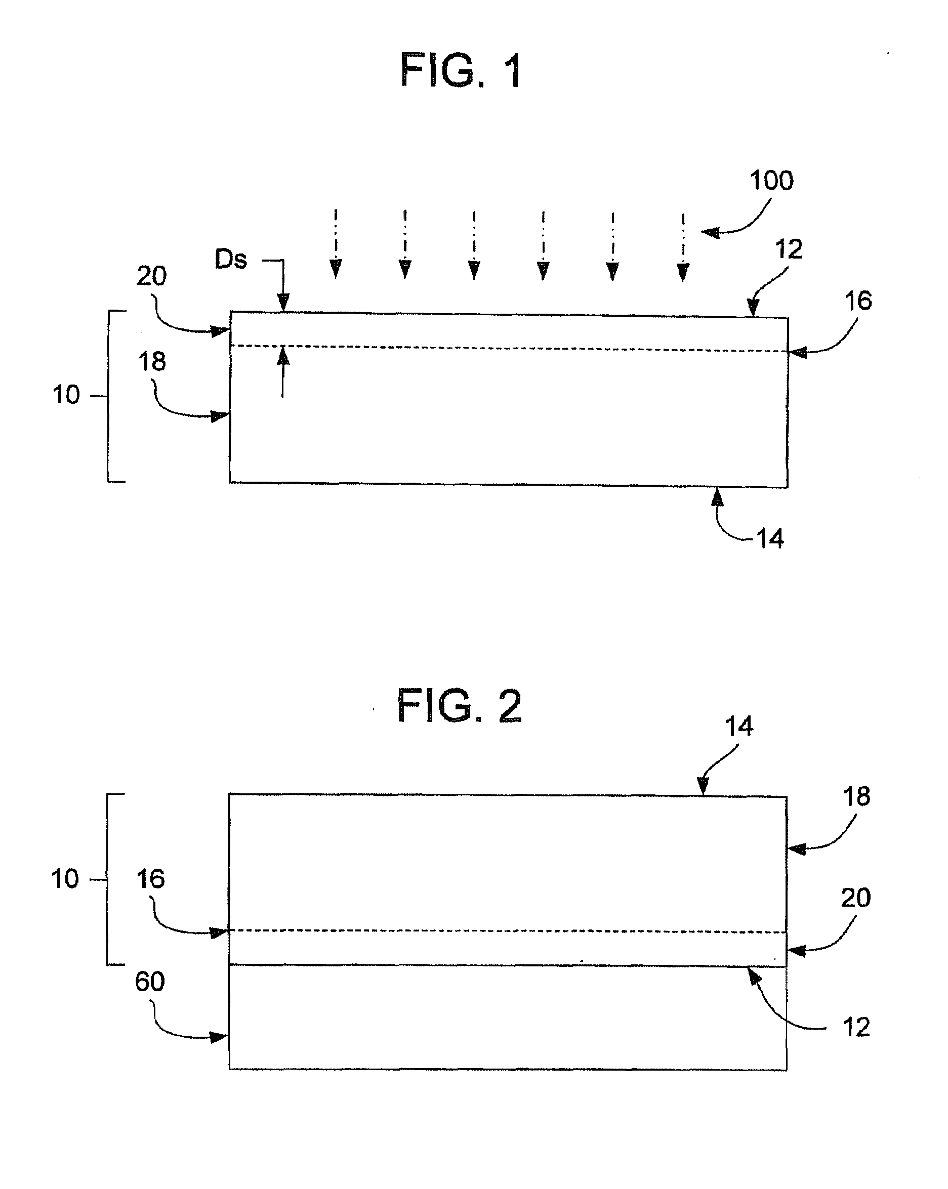
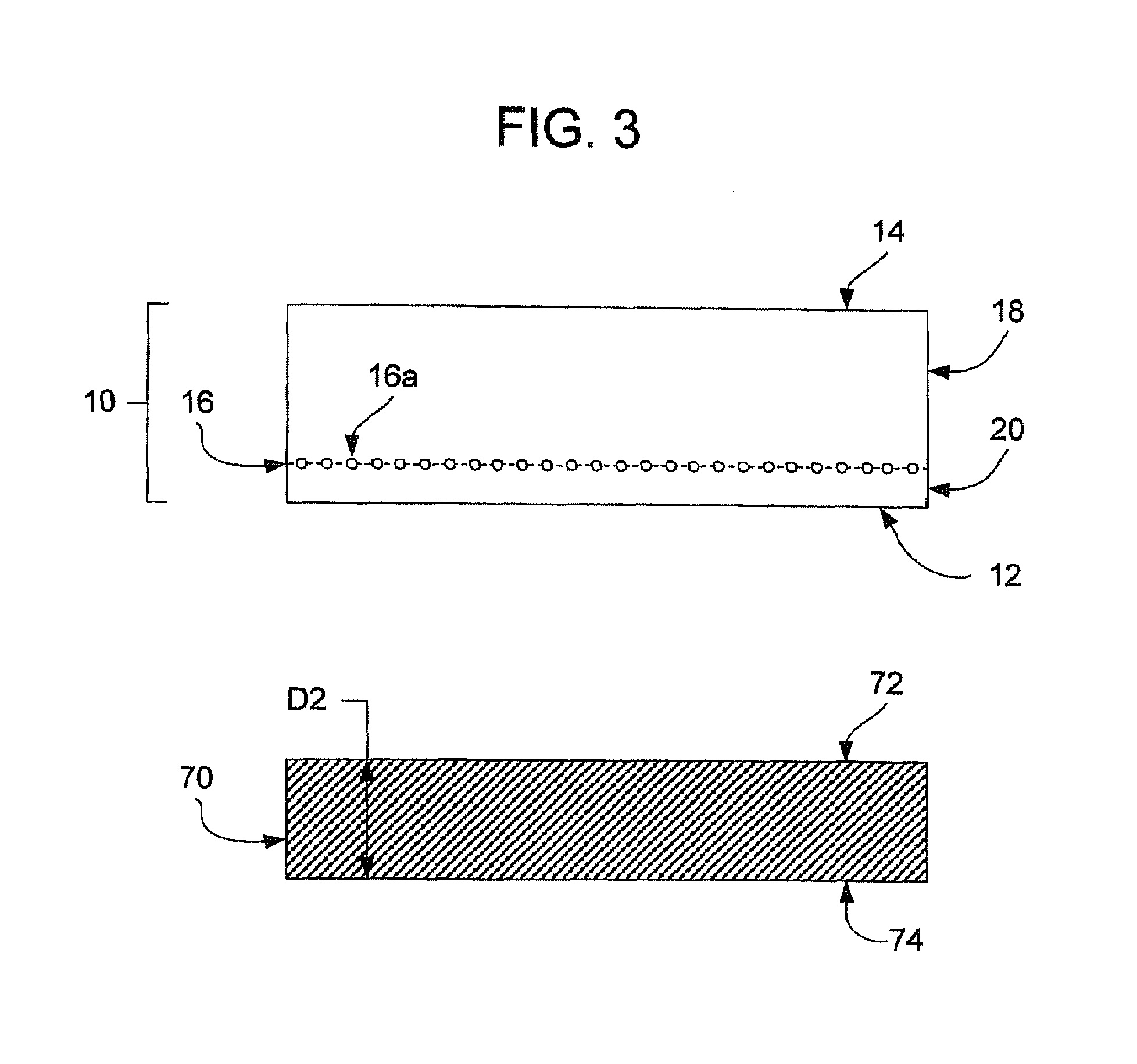
[0048]In this Example, an SCS film is transferred to a polymer substrate in accordance with the present invention. A boron-doped SCS wafer, with a resistivity of 1-10 ohm-cm and thickness of about 500 microns was hydrogen ion-implanted at 100 KeV and 8×10¹⁶ ions / cm2 dosage. The ion-implanted silicon wafer was heat-treated in air at 450° C. for about one hour on a smooth glass support and then allowed to cool to about room temperature. A polysulfone film with a thickness of about 1 millimeter was placed on a surface heated to about 225° C. and the film was allowed to heat to temperature. The cooled silicon wafer was carefully removed from the smooth glass support and placed on the heated polysulfone film, with the implanted side of the silicon wafer contacting the polysulfone film. A load of about 1 psi was placed on the silicon wafer and polysulfone film for about 30 minutes. The heat was turned off and the silicon wafer and polysulfone film were allowed to cool to about ambient tem...

example 2

[0050]For comparison, an attempt was made to transfer an SCS film to a polymer substrate without first heat-treating the ion-implanted silicon wafer on a smooth glass support. In this example, the silicon wafer was implanted as in Example 1. A polysulfone film with a thickness of about 1 millimeter was placed on a surface heated to 225° C. and allowed to heat up to temperature. The ion-implanted silicon wafer was placed on the polysulfone film with the implanted side of the silicon wafer contacting the polysulfone film. A small load of about 1 psi was placed on the silicon wafer and polysulfone film. The temperature was maintained at about 225° C. for about 30 minutes. The silicon wafer and polysulfone film were allowed to cool to about ambient temperature and the load was removed.

[0051]It was found that the silicon wafer and polysulfone film were very strongly bonded and difficult to separate. In forcing the samples apart, the silicon wafer broke, leaving chunks of the wafer bonded...


PUM

PropertyMeasurementUnit
temperatureaaaaaaaaaa

Abstract

Processes for transferring a semiconductor material to a polymer substrate to provide flexible semiconductor material include implanting ions to a predetermined depth in a semiconductor substrate, heat-treating the ion-implanted semiconductor substrate for a period of time and at a temperature effective to cause defect formation and enlargement of the implanted ion defect, adhering the ion-implanted, heat-treated substrate to a polymer substrate, and separating a semiconductor film such as a single crystal silicon film from the semiconductor substrate; and devices having single crystal silicon films disposed directly or indirectly on polymer films.

Description

CROSS-REFERENCE TO RELATED APPLICATIONS[0001]This application claims the benefit of U.S. application Ser. No. 60 / 674,983, filed Apr. 25, 2005 and entitled “Flexible Display Substrates” which is incorporated by reference herein.BACKGROUND OF THE INVENTION[0002]The present invention relates to thin film semiconductors, and in particular, to methods of making thin film semiconductors having a polymer substrate, and structures having a single crystal silicon film and polymer substrate.[0003]There is a growing need for a variety of display devices, such as liquid crystal display (LCD), organic light emitting diode (OLED), and active matrix liquid crystal display (AMLCD) devices. These display devices are based on technology using thin-film semiconductor material. The thin-film semiconductor material is used to produce thin-film transistors (TFT), three-terminal devices in which an input signal controls the output current. TFTs are classified into those using polycrystalline silicon (poly...

Claims


Application Information

Patent Timeline
Patent Type & Authority Applications(United States)
IPC IPC(8): H01L21/18
CPCH01L21/76251Y10T428/12674H01L21/76254B32B15/00H01L21/762
Inventor GADKAREE, KISHOR P.
Owner CORNING INC
Why Eureka
Try Eureka