Electron beam apparatus

a charge-particle, electron-beam technology, applied in the field of charge-particle-beam apparatus, can solve the problems of electron optics producing large off-axis aberrations, mask or wafer damage during semiconductor fabrication process, and electron optics can produce large radiation damage to samples, so as to reduce total emission current, improve imaging resolution, and reduce the effect of electron emission current density without reducing angular intensity

US20100102227A1Inactive Publication Date: 2010-04-29ASML NETHERLANDS BV
49 Cites 38 Cited by

Patent Information

Authority / Receiving Office
US · United States
Current Assignee / Owner
Publication Date
2010-04-29
Estimated Expiration
Not applicable · inactive patent

Smart Images

  • Figure 1
    Figure 1
  • Figure 2
    Figure 2
  • Figure 3
    Figure 3
Patent Text Reader

Abstract

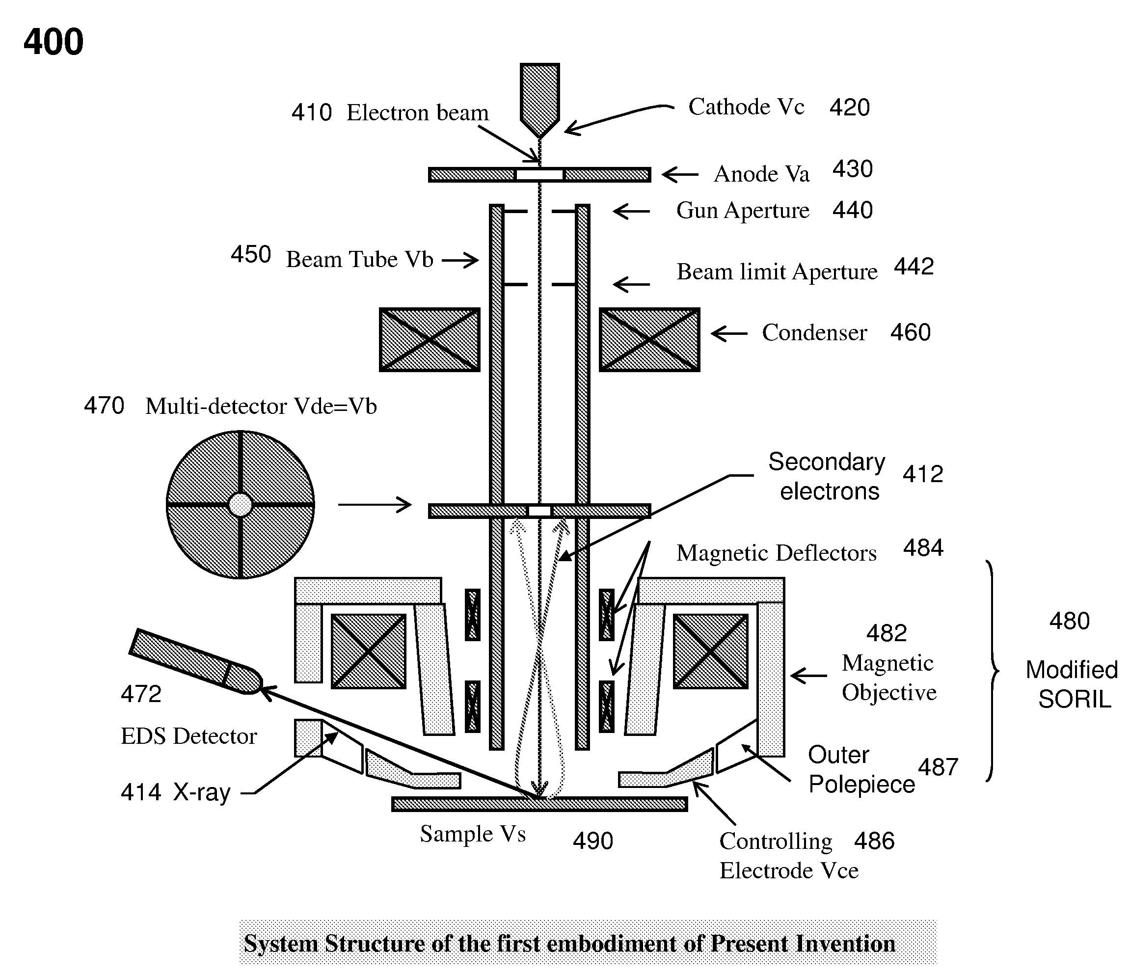
The present invention relates to a charged particle beam apparatus which employs a scanning electron microscope for sample inspection and defect review.The present invent provides solution of improving imaging resolution by utilizing a field emission cathode tip with a large tip radius, applying a large accelerating voltage across ground potential between the cathode and anode, positioning the beam limit aperture before condenser lens, utilizing condenser lens excitation current to optimize image resolution, applying a high tube bias to shorten electron travel time, adopting and modifying SORIL objective lens to ameliorate aberration at large field of view and under electric drifting and reduce the urgency of water cooling objective lens while operating material analysis.The present invent provides solution of improving throughput by utilizing fast scanning ability of SORIL and providing a large voltage difference between sample and detectors.
Need to check novelty before this filing date? Find Prior Art

Description

RELATED APPLICATIONS

[0001] Under 35 USC §120, this application is a Non-Provisional application and is related to co-pending U.S. patent application Ser. No. 12 / 130,879, filed on May 30, 2008, entitled “AN ELECTRON BEAM APPARATUS”; to U.S. patent application Ser. No. 11 / 668,846, filed on Jan. 30, 2007, entitled “CHARGE PARTICLE DETECTION DEVICES, all of which are incorporated herein by reference.FIELD OF THE INVENTION

[0002] The present invention relates to a charged particle beam apparatus which employs a scanning electron microscope for sample inspection and defect review. However, it would be recognized that the invention has a much broader range of applicability.BACKGROUND OF THE INVENTION

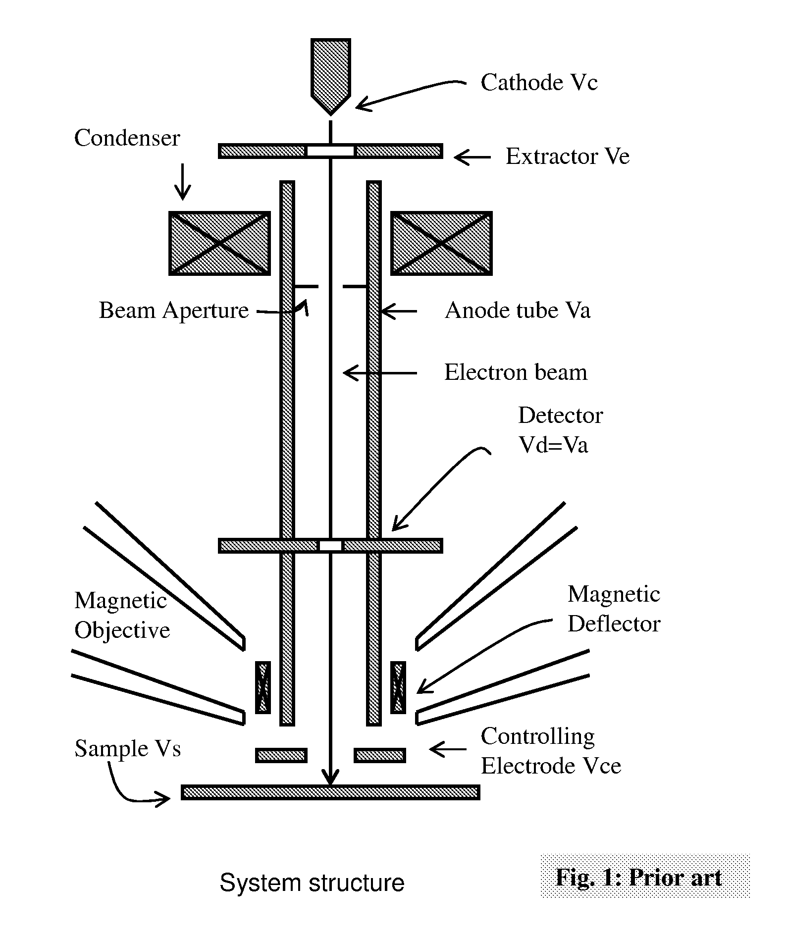
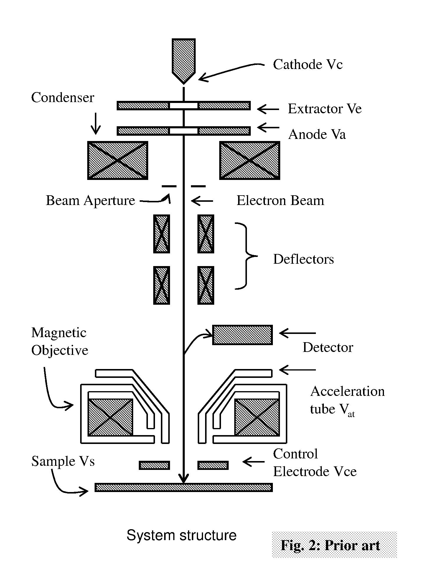
[0003] A charged particle beam apparatus typically employs a scanning electron microscopy (SEM), which is a known technique used in semiconductor manufacturing. Defects can occur on the mask or wafer during the semiconductor fabrication process. These defects impact yield to a great degree. Defect ...

Examples

Embodiment Construction

[0021]Reference will now be made in detail to specific embodiments of the invention. Examples of these embodiments are illustrated in accompanying drawings. While the invention will be described in conjunction with these specific embodiments, it will be understood that it is not intended to limit the invention to these embodiments. On the contrary, it is intended to cover alternatives, modifications, and equivalents as may be included within the spirit and scope of the invention as defined by the appended claims. In the following description, numerous specific details are set forth in order to provide a through understanding of the present invention. The present invention may be practiced without some or all of these specific details. In other instances, well known process operations are not described in detail in order not to unnecessarily obscure the present invention.

[0022]A charged particle beam apparatus which employs a scanning electron microscope for sample inspection and def...