

Differential amplifier circuit amplifying differential signals with selectively switching between differential signals and ad converter apparatus
a technology of differential signal and amplifier circuit, which is applied in the direction of code conversion, instruments, analogue conversion, etc., can solve the problems of linearity deterioration, signal-to-noise power ratio deterioration, and difficulty in realizing high-accuracy analog circuits, so as to improve the snr of the entire ad converter apparatus, improve the snr of the ad converter apparatus, and increase the voltage resolution
- Summary
- Abstract
- Description
- Claims
- Application Information
AI Technical Summary
Benefits of technology
Problems solved by technology
Method used
Image

Examples
first preferred embodiment
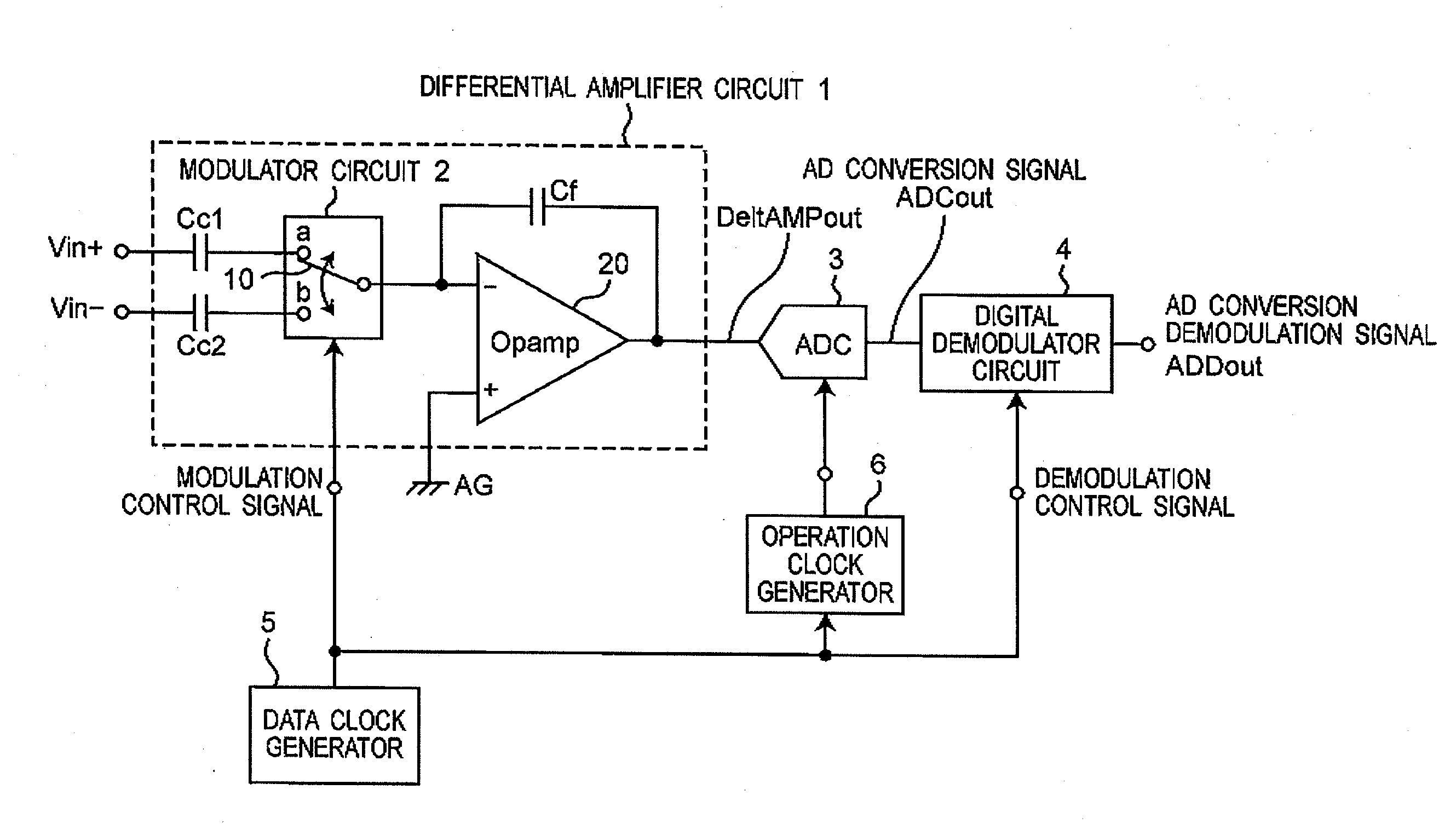
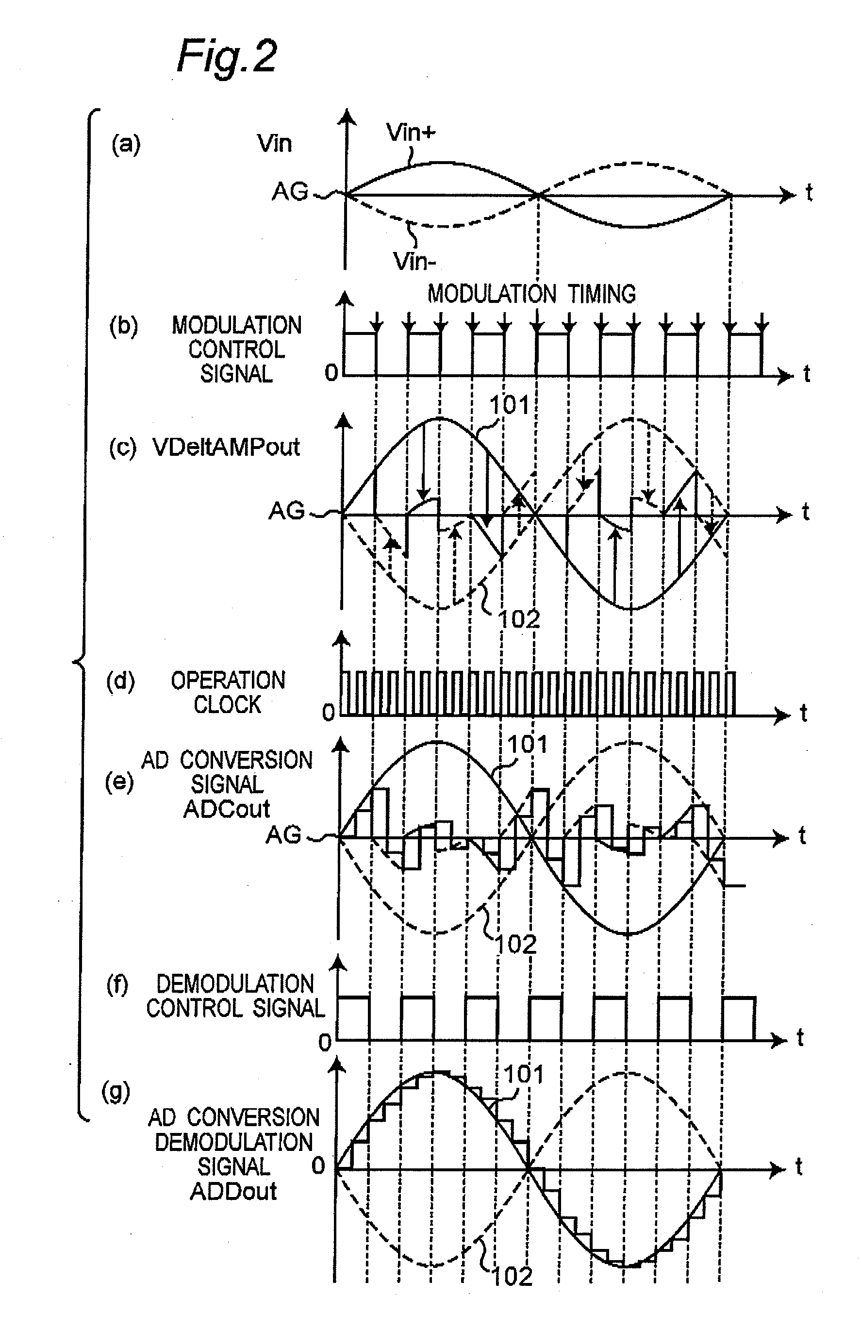
[0054]FIG. 1 is a block diagram showing a configuration of an AD converter apparatus according to a first preferred embodiment of the present invention. In addition, FIG. 2 shows signal waveform charts of signals representing operations of the AD converter apparatus of FIG. 1. More specifically, FIG. 2(a) is a signal waveform chart of analog signals Vin+ and Vin− inputted to a differential amplifier circuit 1 of FIG. 1. FIG. 2(b) is a signal waveform chart of a modulation control signal inputted to the differential amplifier circuit 1 of FIG. 1. FIG. 2(c) is a signal waveform chart of an output signal DeltAMPout from the differential amplifier circuit 1 of FIG. 1. FIG. 2(d) is a signal waveform chart of an operation clock inputted to an AD converter 3 of FIG. 1. FIG. 2(e) is a signal waveform chart of an AD conversion signal ADCout from the AD converter 3. FIG. 2(f) is a signal waveform chart of a demodulation control signal inputted to a digital demodulator circuit 4 of FIG. 1. FIG...
second preferred embodiment
[0064]FIG. 3 is a block diagram showing a configuration of an AD converter apparatus according to a second preferred embodiment of the present invention. FIG. 4 is a block diagram showing a configuration of a modulation control circuit 22 of FIG. 3. In addition, FIG. 5 shows signal waveform charts of signals representing operations of the AD converter apparatus of FIG. 3. More specifically, FIG. 5(a) is a signal waveform chart of analog signals Vin+ and Vin− inputted to a differential amplifier circuit 1 of FIG. 3. FIG. 5(b) is a signal waveform chart of an output signal DeltAMPout from the differential amplifier circuit 1 of FIG. 3. FIG. 5(c) is a signal waveform chart of an output signal Compout2 from a comparator circuit 21-2 of FIG. 3. FIG. 5(d) is a signal waveform chart of an output signal Compout1 from a comparator circuit 21-1 of FIG. 3. FIG. 5(e) is a signal waveform chart of an AT conversion signal ATCout and a modulation control signal from the modulation control circuit ...
third preferred embodiment
[0088]FIG. 6 is a block diagram showing a configuration of an AD converter apparatus according to a third preferred embodiment of the present invention. FIG. 7 shows signal waveform charts of signals representing operations of the AD converter apparatus of FIG. 6. More specifically, FIG. 7(a) is a signal waveform chart of analog signals Vin.+ and Vin− inputted to a differential amplifier circuit 1 of FIG. 6. FIG. 7(b) is a signal waveform chart of an output signal DeltAMPout from the differential amplifier circuit 1 of FIG. 6. FIG. 7(c) is a signal waveform chart of an output signal Compout2 from a comparator circuit 21-2 of FIG. 6. FIG. 7(d) is a signal waveform chart of an output signal Compout1 from a comparator circuit 21-1 of FIG. 6. FIG. 7(e) is a signal waveform chart of an output signal Compoutmn from a comparator circuit 23-n (n=1, 2, . . . , N) of FIG. 6. FIG. 7(f) is a signal waveform chart of an AT conversion signal ATCout and a modulation control signal from a modulatio...
PUM
 Abstract
Description
Claims
Application Information