Semiconductor device and method for manufacturing the same

Active Publication Date: 2010-05-06
SEMICON ENERGY LAB CO LTD
View PDF101 Cites 121 Cited by
  • Summary
  • Abstract
  • Description
  • Claims
  • Application Information

AI Technical Summary

Benefits of technology

[0022]According to an embodiment of the present invention, in a thin film transistor using an oxide semiconductor layer, a semiconductor layer having higher electrical conductivity and a smaller thickness than the oxide semiconductor layer is formed between the oxide semiconductor layer and a gate insulating layer, whereby field effect mobility of the thin film transistor can

Problems solved by technology

On the other hand, although a thin film transistor using polycrystalline silicon has high field effect mobility, it takes an enormous amount of time to form the thin film

Method used


Image

  • Semiconductor device and method for manufacturing the same
  • Semiconductor device and method for manufacturing the same
  • Semiconductor device and method for manufacturing the same

Examples


embodiment 1

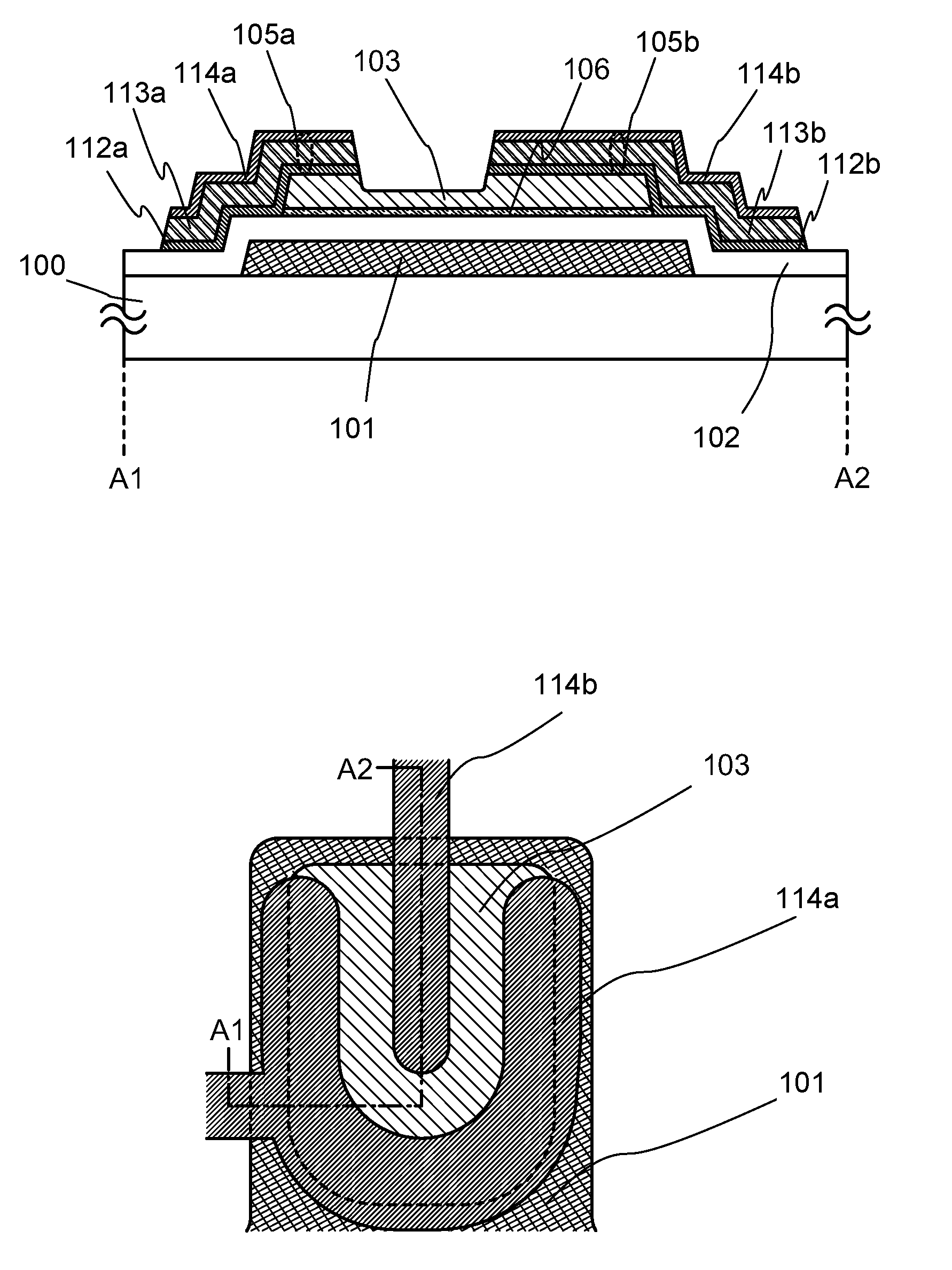
[0054]In this embodiment, a structure of a thin film transistor is described with reference to FIGS. 1A and 1B.

[0055]A thin film transistor having a bottom gate structure of this embodiment is illustrated in FIGS. 1A and 1B. FIG. 1A is a cross-sectional view, and FIG. 1B is a plan view. FIG. 1A is a cross-sectional view along line A1-A2 of FIG. 1B.

[0056]In the thin film transistor illustrated in FIGS. 1A and 1B, a gate electrode layer 101 is provided over a substrate 100; a gate insulating layer 102 is provided over the gate electrode layer 101; a semiconductor layer 106 is provided over the gate insulating layer 102; an oxide semiconductor layer 103 is provided over the semiconductor layer 106; and a source and drain electrode layers 105a and 105b are provided over the oxide semiconductor layer 103.

[0057]The gate electrode layer 101 can be formed to have a single-layer structure or a stacked-layer structure using a metal material such as aluminum, copper, molybdenum, titanium, chro...

embodiment 2

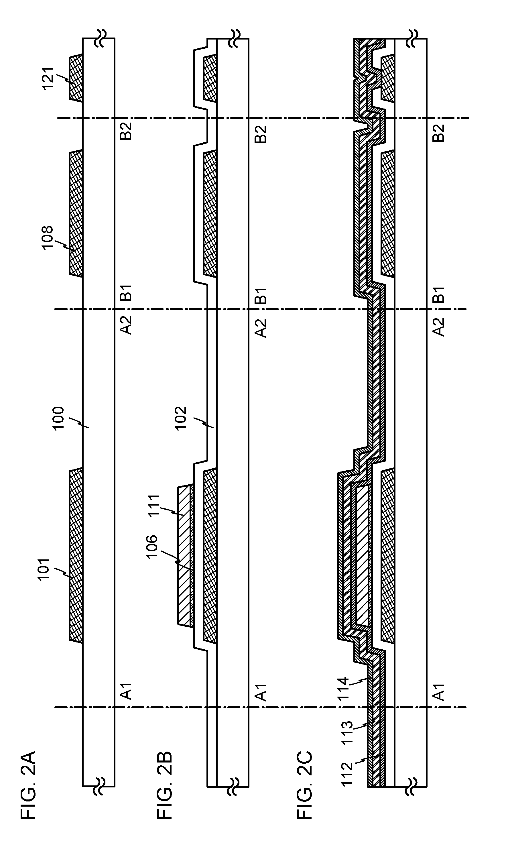
[0070]In this embodiment, a manufacturing process of a display device including the thin film transistor described in Embodiment 1 will be described with reference to FIGS. 2A to 2C, FIGS. 3A to 3C, FIG. 4, FIG. 5, FIG. 6, FIG. 7, FIGS. 8A-1 to 8B-2, and FIG. 9. FIGS. 2A to 2C and FIGS. 3A to 3C are cross-sectional views, and FIG. 4, FIG. 5, FIG. 6, and FIG. 7 are plan views. Line A1-A2 and line B1-B2 in each of FIG. 4, FIG. 5, FIG. 6, and FIG. 7 correspond to line A1-A2 and line B1-B2 in each of the cross-sectional views of FIGS. 2A to 2C and FIGS. 3A to 3C, respectively.

[0071]First, the substrate 100 is prepared. As the substrate 100, any of the following substrates can be used: non-alkaline glass substrates made of barium borosilicate glass, aluminoborosilicate glass, aluminosilicate glass, and the like by a fusion method or a float method; ceramic substrates; plastic substrates having heat resistance enough to withstand a process temperature of this manufacturing process;

[0072]a...

embodiment 3

[0128]In this embodiment, a thin film transistor having a different structure than that of the thin film transistor described in Embodiment 1 is described with reference to FIG. 10.

[0129]A thin film transistor having a bottom gate structure of this embodiment is illustrated in FIG. 10. In the thin film transistor illustrated in FIG. 10, the gate electrode layer 101 is provided over the substrate 100; the gate insulating layer 102 is provided over the gate electrode layer 101; the semiconductor layer 106 is provided over the gate insulating layer 102; the oxide semiconductor layer 103 is provided over the semiconductor layer 106; buffer layers 301a and 301b are provided over the oxide semiconductor layer 103; and the source and drain electrode layers 105a and 105b are provided over the buffer layers 301a and 301b. The source or drain electrode layer 105a has a three-layer structure of the first conductive layer 112a, the second conductive layer 113a, and the third conductive layer 11...


PUM


Abstract

An object is to improve field effect mobility of a thin film transistor using an oxide semiconductor. Another object is to suppress increase in off current even in a thin film transistor with improved field effect mobility. In a thin film transistor using an oxide semiconductor layer, by forming a semiconductor layer having higher electrical conductivity and a smaller thickness than the oxide semiconductor layer between the oxide semiconductor layer and a gate insulating layer, field effect mobility of the thin film transistor can be improved, and increase in off current can be suppressed.

Description

BACKGROUND OF THE INVENTION[0001]1. Field of the Invention[0002]The present invention relates to a semiconductor device using an oxide semiconductor, a display device using the semiconductor device, and a manufacturing method thereof.[0003]2. Description of the Related Art[0004]In recent years, liquid crystal display devices typified by liquid crystal displays are becoming widespread. As a liquid crystal display, an active matrix liquid crystal display device provided with pixels each including a thin film transistor (TFT) is often used. In a thin film transistor included in an active matrix liquid crystal display device, amorphous silicon or polycrystalline silicon is used as an active layer. Although a thin film transistor using amorphous silicon has low field effect mobility, it can be easily formed over a large-sized substrate such as a large glass substrate. On the other hand, although a thin film transistor using polycrystalline silicon has high field effect mobility, it takes...

Claims


Application Information

Patent Timeline
IPC IPC(8): H01L29/786H01L21/336
CPCH01L27/1225H01L29/78618H01L29/7869H01L29/78696H01L29/78693H01L29/66969H01L29/66742H01L29/24H01L29/04H01L27/1259H01L27/1248H01L29/42356G02F1/1368G02F1/167H01L27/3262H01L27/127H01L29/45H01L29/41733H10K59/1213
Inventor AKIMOTO, KENGOSASAKI, TOSHINARI
Owner SEMICON ENERGY LAB CO LTD
Why Eureka
Try Eureka