Gallium nitride semiconductor device and method for producing the same

a technology of gallium nitride and semiconductor devices, which is applied in the direction of semiconductor devices, basic electric elements, electrical equipment, etc., can solve the problems of difficult to reduce the total size of the switching circuit, limited use of normal on-type gan semiconductor elements, and limited distance between adjacent ones of semiconductor switches, so as to reduce the total size of the circuit in which the first and second semiconductor elements are mounted, the effect of suppressing the lowering of the operating speed and reducing the power loss and cos

Active Publication Date: 2010-05-06
FUJI ELECTRIC CO LTD
View PDF3 Cites 25 Cited by
  • Summary
  • Abstract
  • Description
  • Claims
  • Application Information

AI Technical Summary

Benefits of technology

[0029]According to the invention, because the first and second semiconductor elements are formed in one semiconductor device, the total size of a circuit in which the first and second semiconductor elements are mounted can be reduced greatly. Moreover, because the whole of the circuit can be formed of gallium nitride semiconductor elements, the semiconductor device can be used under a high temperature environment compared with the case where a circuit formed of Si semiconductor elements is used. Moreover, because external components such as external wiring can be dispensed with, lowering of the operating speed can be suppressed to attain reduction in power loss and cost. Moreover, because the second semiconductor element can be formed to have substantially the same structure as that of the first semiconductor element, the semiconductor device can be produced with little increase in the number of production steps. Accordingly, the production cost can be greatly reduced. Because the second semiconductor layer is formed by epitaxial growth, the channel mobility of the second semiconductor layer can be set to be substantially the same as the channel mobility of a single crystal layer. Moreover, because the third semiconductor layer is formed by epitaxial growth, the third semiconductor layer can be formed as a first conductivity type high concentration region.
[0030]According to the sixth configuration of the invention, in the first semiconductor element, a drain electrode is formed on a rear surface of the semiconductor substrate and a short-circuit electrode extending from the first semiconductor layer but not piercing the semiconductor substrate is provided so that a current can flow into the semiconductor substrate from the first source region provided on the second semiconductor layer. Moreover, because a high concentration semiconductor region is provided in a boundary between the first semiconductor layer and the short-circuit electrode so as to be contacted to the short-circuit electrode, a current flowing in the first semiconductor layer can be collected to the short-circuit electrode. Accordingly, the first semiconductor element can be formed as a quasi-vertical structure. Therefore, an electrode pad etc. provided on a front surface of the semiconductor element so as to be connected to the drain electrode of the first semiconductor element becomes unnecessary, so that the region for the unnecessary electrode pad, etc. can be reduced.
[0031]The gallium nitride semiconductor device and the method of producing the same according to the invention have an effect of reducing the total size of a circuit in which semiconductor elements are provided. There is another effect that cost can be reduced. There is a further effect that the semiconductor device can be used under a high temperature environment.

Problems solved by technology

The normally-on type GaN semiconductor element however has limited uses.
However, because the semiconductor switches are formed separately in semiconductor devices 1100 to 1300 respectively, the distance between adjacent ones of the semiconductor switches is limited, for example, by the size of a mount region or each semiconductor device in a printed substrate.
For this reason, it is difficult to reduce the total size of the switching circuit even if the GaN semiconductor element were used as a semiconductor switch.
Moreover, there is a problem of signal delay due to external wiring or malfunction caused by production of noise.

Method used


Image

  • Gallium nitride semiconductor device and method for producing the same
  • Gallium nitride semiconductor device and method for producing the same
  • Gallium nitride semiconductor device and method for producing the same

Examples


embodiment 1

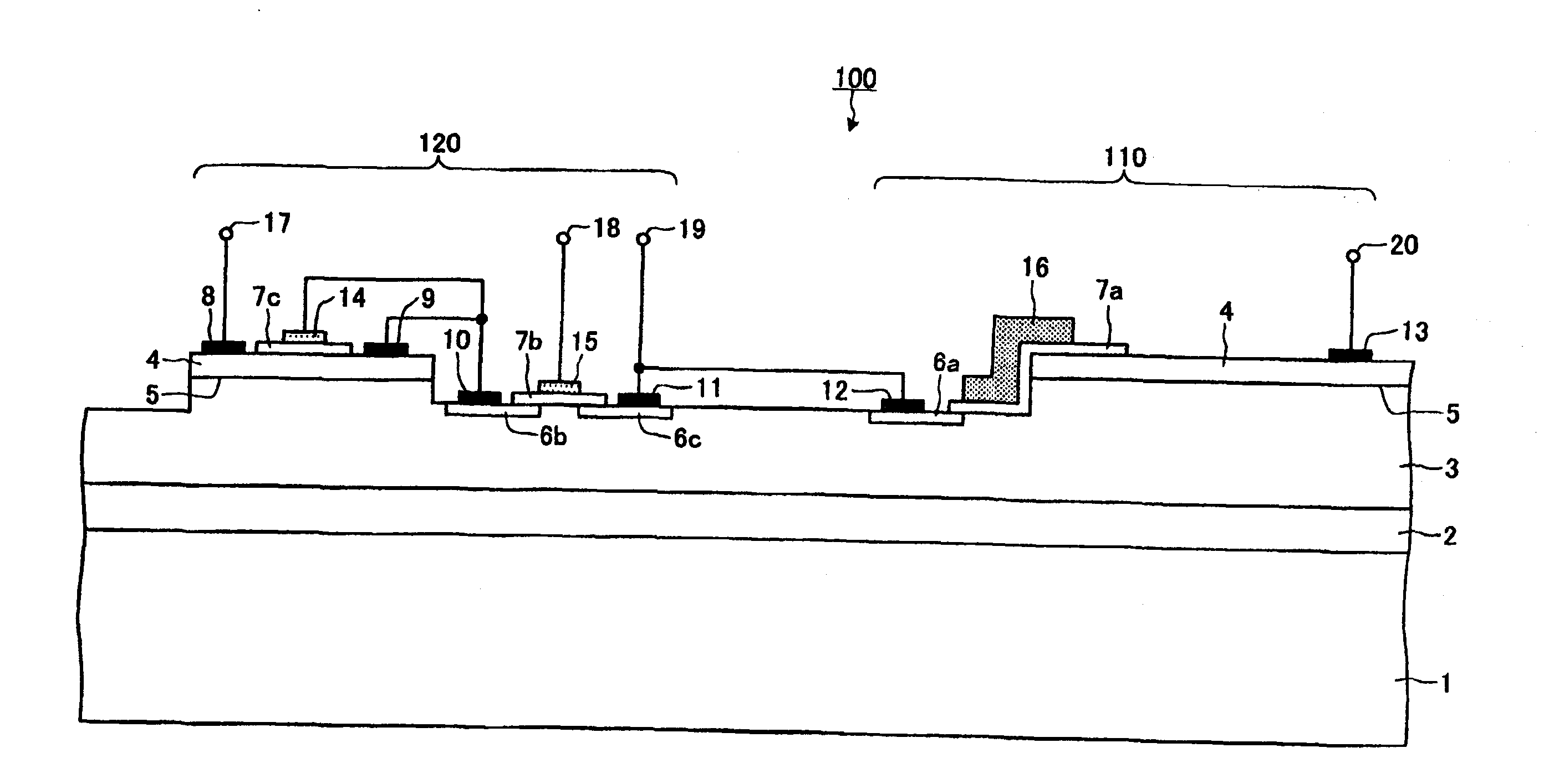
[0049]FIG. 1 is a sectional view showing a semiconductor device according to Embodiment 1. In semiconductor device 100 shown in FIG. 1, insulating layer 2 is provided on a surface of semiconductor substrate 1. Undoped or n-type first GaN layer 3 (first semiconductor layer) is provided on a surface of insulating layer 2. AlGaN layer 4 (second semiconductor layer) is provided on part of a surface of first GaN layer 3. Surface barrier layer 5 formed by a two-dimensional electron gas is provided in an interface between first GaN layer 3 and AlGaN layer 4. A first recess which is dented but does not pierce first GaN layer 3 is provided in a region of first GaN layer 3 where AlGaN layer 4 is not provided. End portions of AlGaN layer 4 and surface barrier layer 5 are exposed on side wall portions of the first recess.

[0050]First high withstand voltage transistor 110 (first semiconductor element) and control circuit 120 (second semiconductor element) are formed integrally on the aforemention...

embodiment 2

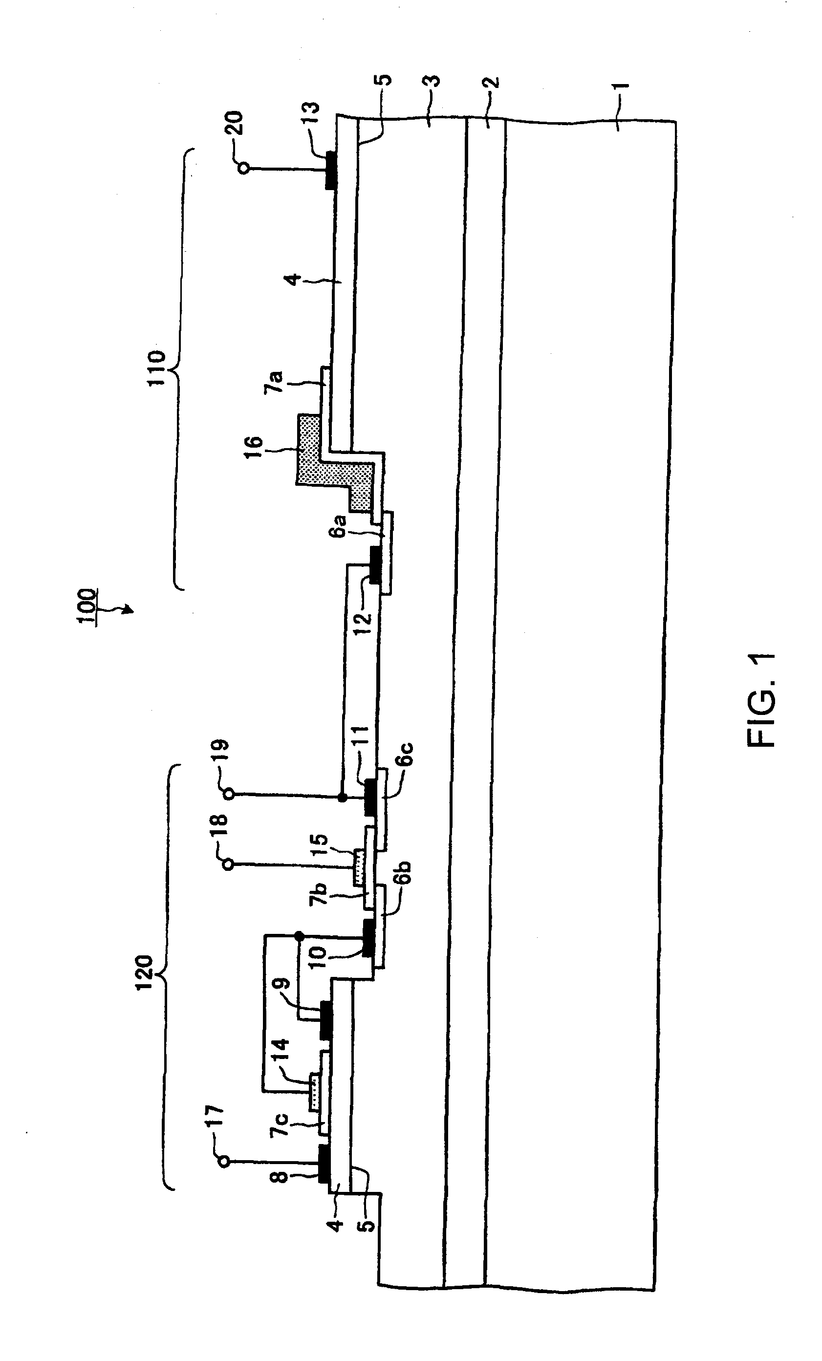
[0058]FIG. 2 is a sectional view showing a semiconductor device according to Embodiment 2. A p-channel MOSFET (first conductivity type insulated gate field effect transistor) is provided in place of the depression type n-channel MOSFET of control circuit 120 in Embodiment 1. Each of first high withstand voltage transistor 110 and the p-channel MOSFET is formed in a structure without use of surface barrier layer 5 formed by two-dimensional electron gas.

[0059]Like Embodiment 1, insulating layer 2 is provided on a surface of semiconductor substrate 1. P-type (first conductivity type) first GaN layer 3 (first semiconductor layer) is provided on a surface of insulating layer 2. N-type (second conductivity type) second GaN layer 30 (second semiconductor layer) is provided on part of a surface of first GaN layer 3. P-type high concentration GaN layer 31 (third semiconductor layer) is provided on part of a surface of second GaN layer 30. Like Embodiment 1, a first recess which is dented but...

embodiment 3

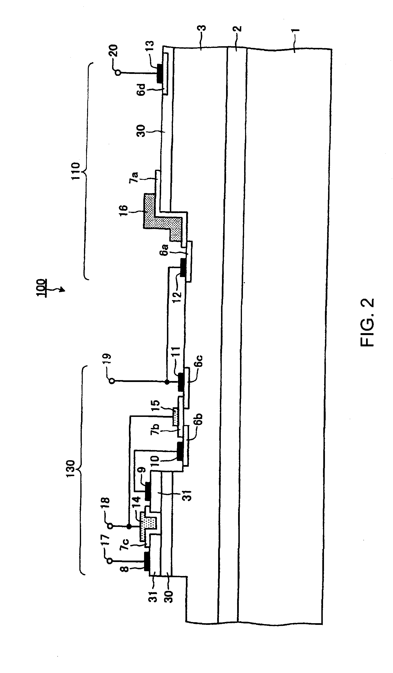
[0065]FIG. 3 is a sectional view showing a semiconductor device according to Embodiment 3. Insulating region 32 may be formed in first GaN layer 3 between first high withstand voltage transistor110 and control circuit 130 in Embodiment 2, that is, insulating region 32 may be formed between the first element region and the second element region to obtain a structure in which first high withstand voltage transistor 110 and control circuit 130 are electrically insulated from each other.

[0066]The structure of first high withstand voltage transistor 110 and control circuit 130 is the same as in Embodiment 2. Insulating region 32 is formed in first GaN layer 3 so as to pierce first GaN layer 3 between first high withstand voltage transistor 110 and control circuit 130. Insulating region 32 may be provided as a region having first GaN layer 3 partially removed. Alternatively, insulating region 32 may be provided as a region filled with an insulating substance such as silicon dioxide (SiO2)...


PUM


Abstract

An insulating layer, an undoped first GaN layer and an AlGaN layer are laminated in this order on a surface of a semiconductor substrate. A surface barrier layer formed by a two-dimensional electron gas is provided in an interface between the first GaN layer and the AlGaN layer. A recess (first recess) which reaches the first GaN layer but does not pierce the first GaN layer is formed in a surface layer of the AlGaN layer. A first high withstand voltage transistor and a control circuit are formed integrally on the aforementioned semiconductor substrate. The first high withstand voltage transistor is formed in the first recess and on a surface of the AlGaN layer. The control circuit includes an n-channel MOSFET formed in part of the first recess, and a depression type n-channel MOSFET formed on a surface of the AlGaN layer. In this manner, there are provided a gallium nitride semiconductor device which can be used under a high temperature environment while reduction in total circuit size can be attained, and a method for producing the gallium nitride semiconductor device.

Description

BACKGROUND OF THE INVENTION[0001]A. Field of the Invention[0002]The present invention relates to a gallium nitride semiconductor device and a method for producing the same.[0003]B. Description of the Related Art[0004]A gallium nitride (GaN) compound semiconductor (hereinafter referred to as GaN semiconductor element) has been heretofore used as a semiconductor material of a semiconductor element for high-frequency device use. In the GaN semiconductor element, a buffer layer and a doped GaN layer, for example, formed by a metal organic chemical vapor deposition (MOCVD) method are provided on a surface of a semiconductor substrate.[0005]FIG. 14 is a sectional view showing a lateral structure gallium nitride semiconductor element according to the background art. As shown in FIG. 14, in the lateral structure GaN semiconductor element, a buffer layer 1002, silicon-doped n-type GaN layer 1003 and aluminum gallium nitride (AlGaN) layer 1004 are laminated in this order on a surface of semic...

Claims


Application Information

Patent Timeline
Patent Type & Authority Applications(United States)
IPC IPC(8): H01L29/20H01L21/20
CPCH01L21/743H01L21/8258H01L29/0649H01L29/0847H01L29/7788H01L29/42356H01L29/66462H01L29/7787H01L29/2003
Inventor UENO, KATSUNORI
Owner FUJI ELECTRIC CO LTD
Why Eureka
Try Eureka