High density spin-transfer torque MRAM process

a high-density spin-transfer torque and mram technology, applied in the manufacture/treatment of galvano-magnetic devices, semiconductor devices, electrical equipment, etc., can solve the problems of destroying alox, mgo, or the like thin insulating barrier, and the fundamental limitation of scalability of conventional mram, so as to reduce the problem of defects

Active Publication Date: 2010-05-06
TAIWAN SEMICON MFG CO LTD
View PDF12 Cites 60 Cited by
  • Summary
  • Abstract
  • Description
  • Claims
  • Application Information

AI Technical Summary

Benefits of technology

[0012]One objective of the present invention is to provide an integration scheme for a STT-MRAM device that redu

Problems solved by technology

However, conventional MRAM has a fundamental limitation of scalability.
This high current density, which is required to induce the spin-transfer effect, could destroy a thin insulating barrier made of AlOx, MgO, or the like.
The fabrication process of a STT-MRAM is very challengi

Method used


Image

  • High density spin-transfer torque MRAM process
  • High density spin-transfer torque MRAM process
  • High density spin-transfer torque MRAM process

Examples


Embodiment Construction

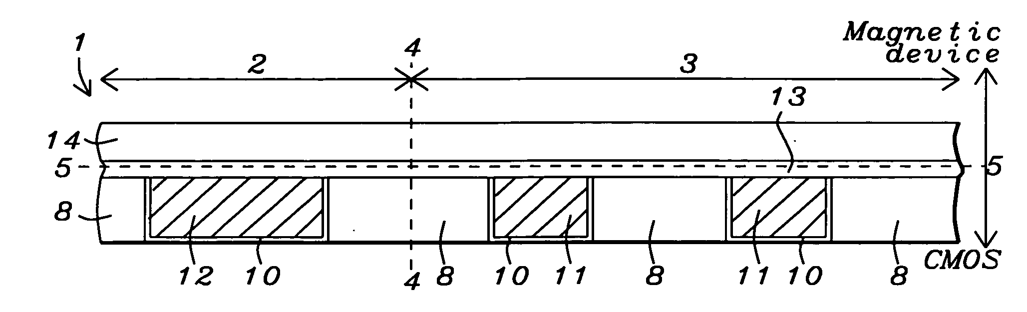
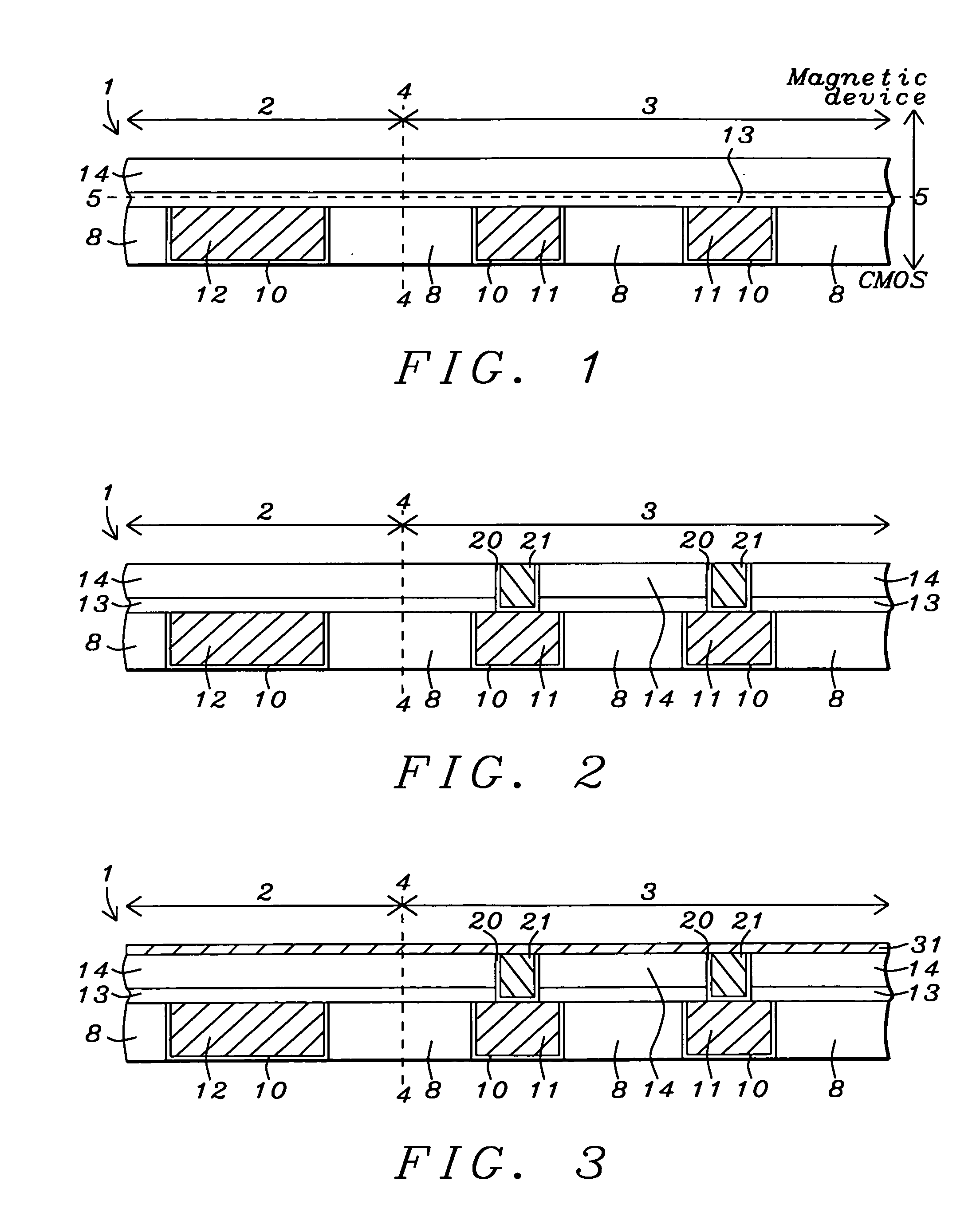
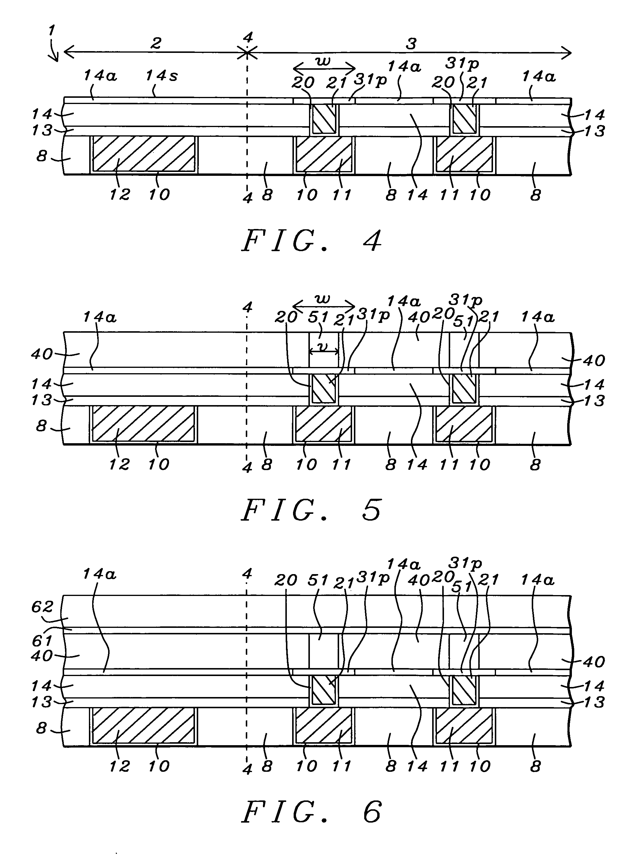
[0026]The present invention is an integration scheme for fabricating a STT-MRAM device that can significantly improve final production yield. The integration scheme includes a process flow that can be readily implemented in a manufacturing environment. Although the exemplary embodiment describes a bottom spin valve MTJ element, the present invention also encompasses other STT-MRAM designs including dual spin valve (DSF) configurations and top spin valve elements. The drawings are not necessarily drawn to scale and the relative sizes of various elements may differ from those in an actual device.

[0027]A method of forming a STT-MRAM structure according to one embodiment of the present invention will now be described. Referring to FIG. 1, a partially completed STT-MRAM structure 1 is shown that includes a substrate comprised of a first dielectric layer 8 and an uppermost CMOS metal layer that includes a plurality of CMOS metal landing pads 11 in a device region 3 and a plurality of CMOS...


PUM


Abstract

A STT-MRAM integration scheme is disclosed wherein the connection between a MTJ and CMOS metal is simplified by forming an intermediate via contact (VAC) on a CMOS landing pad, a metal (VAM) pad that contacts and covers the VAC, and a MTJ on the VAM. A dual damascene process is performed to connect BIT line metal to CMOS landing pads through VAC/VAM/MTJ stacks in a device region, and to connect BIT line connection pads to CMOS connection pads through BIT connection vias outside the device region. The VAM pad is a single layer or composite made of Ta, TaN, or other conductors which serves as a diffusion barrier, has a highly smooth surface for MTJ formation, and provides excellent selectivity with refill dielectric materials during a chemical mechanical polish process. Each VAC is from 500 to 3000 Angstroms thick to minimize additional circuit resistance and minimize etch burden.

Description

RELATED PATENT APPLICATION[0001]This application is related to the following: Docket #HMG07-026, Ser. No. 11 / 975,045, filing date Oct. 17, 2007; assigned to a common assignee and herein incorporated by reference in its entirety.FIELD OF THE INVENTION[0002]The invention relates to an integration scheme for a high density spin-transfer torque (STT) MRAM device and a method of forming the same that significantly improves final production yield and simplifies overall integration capability.BACKGROUND OF THE INVENTION[0003]Magnetoresistive Random Access Memory (MRAM), based on the integration of silicon based Complementary Silicon-Oxide Semiconductor (CMOS) with magnetic tunnel junction (MTJ) technology, is now a proven non-volatile memory technology with many advantages in terms of writing / read speed, power consumption, and lifetime over other commercialized memory types including SRAM, DRAM, Flash, etc. However, conventional MRAM has a fundamental limitation of scalability. STT-MRAM no...

Claims


Application Information

Patent Timeline
IPC IPC(8): H01L29/82H01L21/00
CPCH01L27/228H01L43/12H10B61/22H10N50/01
Inventor ZHONG, TOMTORNG, CHYU-JIUHXIAO, RONGFUZHONG, ADAMKAN, WAI-MING JOHNSONLIU, DANIEL
Owner TAIWAN SEMICON MFG CO LTD
Why Eureka
Try Eureka