Semiconductor device and manufacturing method thereof

a technology of semiconductor devices and manufacturing methods, applied in semiconductor devices, semiconductor/solid-state device details, electrical apparatus, etc., can solve the problems of increasing the chip size, unable to apply construction, and difficulty in performing a loading method of directly connecting the lower surface of the soi substrate to the lead frame, etc., to achieve the effect of reducing the number of manufacturing steps of the wafer manufacturing process, reducing the cost of manufacturing, and increasing the chip siz

Active Publication Date: 2010-05-06
LAPIS SEMICON CO LTD
View PDF4 Cites 28 Cited by
  • Summary
  • Abstract
  • Description
  • Claims
  • Application Information

AI Technical Summary

Benefits of technology

[0010]Because the substrate potential fixing electrode is formed at the upper (front) surface of the SOI layer, it is not possible to apply the construction disclosed in Japanese Patent Application Kokai No. 11-354631 to a package having the external terminal at the lower (back) surface of the SOI substrate without modification. That is, when the structure disclosed in Japanese Patent Application Kokai No. 11-354631 is applied to the W-CSP having the through via, it is necessary to provide a voltage application path different from the through via so as to apply potential to the substrate potential fixing electrode formed at the upper (front) surface of the chip. For example, it is necessary to perform wire bonding. As a result, merits obtained through the adoption of the through via structure are reduced. Furthermore, it is necessary to form a contact, such that the contact reaches the silicon substrate layer, by etching the SOI substrate from the upper face side thereof. As a result, the number of manufacturing steps of the wafer manufacturing process is increased. Also, it is necessary to secure an additional space necessary to form the contact, with the result that the chip size may be increased.
[0011]One object of the present invention is to provide a W-CSP type semiconductor device including an SOI device with a through via. This semiconductor device is capable of fixing potential of a silicon substrate layer of an SOI substrate without increasing a package size or changing a package manufacturing process and a wafer manufacturing process.
[0012]Another object of the present invention is to provide a W-CSP semiconductor device manufacturing method that can fix potential of a silicon substrate layer of an SOI substrate without increasing a package size or changing a package manufacturing process and a wafer manufacturing process.

Problems solved by technology

Thus, it is difficult to perform a loading method of directly connecting the lower surface of the SOI substrate to the lead frame.
In other words, it is not possible to apply the construction disclosed in Japanese Patent Application Kokai No. 7-335811 to the W-CSP having the through via.
Because the substrate potential fixing electrode is formed at the upper (front) surface of the SOI layer, it is not possible to apply the construction disclosed in Japanese Patent Application Kokai No. 11-354631 to a package having the external terminal at the lower (back) surface of the SOI substrate without modification.
Also, it is necessary to secure an additional space necessary to form the contact, with the result that the chip size may be increased.

Method used


Image

  • Semiconductor device and manufacturing method thereof
  • Semiconductor device and manufacturing method thereof
  • Semiconductor device and manufacturing method thereof

Examples


first embodiment

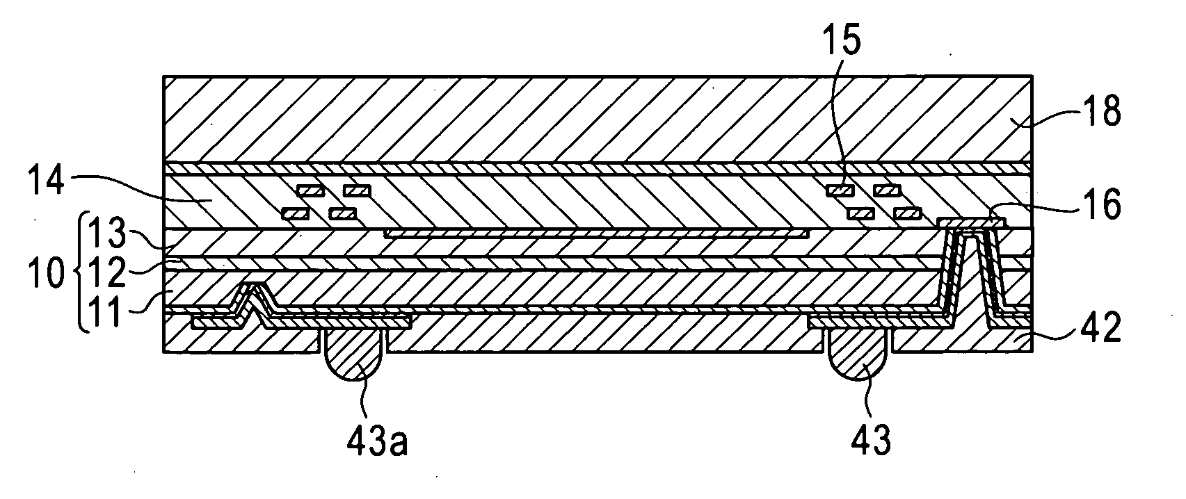
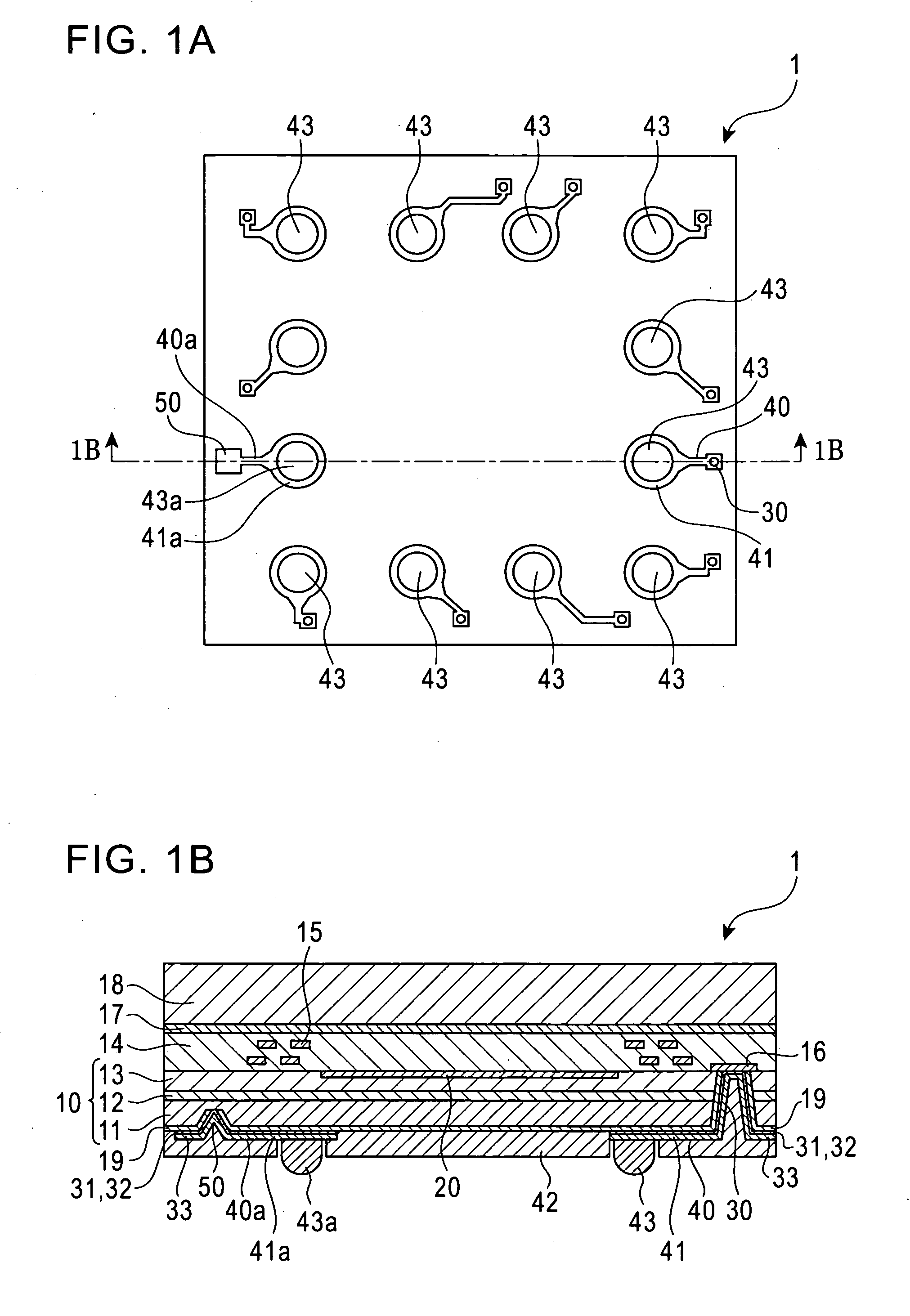
[0059]Referring to FIGS. 1A and 1B, a wafer level chip size package (W-CSP) type image sensor 1 having through vias according to a first embodiment of the present invention will be described.

[0060]A silicon on insulator (SOI) substrate 10 is constructed in a three-layered structure including a silicon substrate layer 11, a buried oxide film layer (BOX layer) 12, and a thin film silicon layer (SOI layer) 13. A sensor circuit 20 including a charge coupled device (CCD) sensor or a complementary metal oxide semiconductor (CMOS) sensor is formed at the upper surface of the SOI layer 13. The upper surface of the SOI layer 13 serves as a light receiving surface. A plurality of imaging devices corresponding to the number of pixels are formed on the SOI layer 13. Light radiated from an object or target is focused on the light receiving surface by an optical system, such as a lens, provided outside the device. Each of the imaging devices outputs a photoelectric conversion signal corresponding...

second embodiment

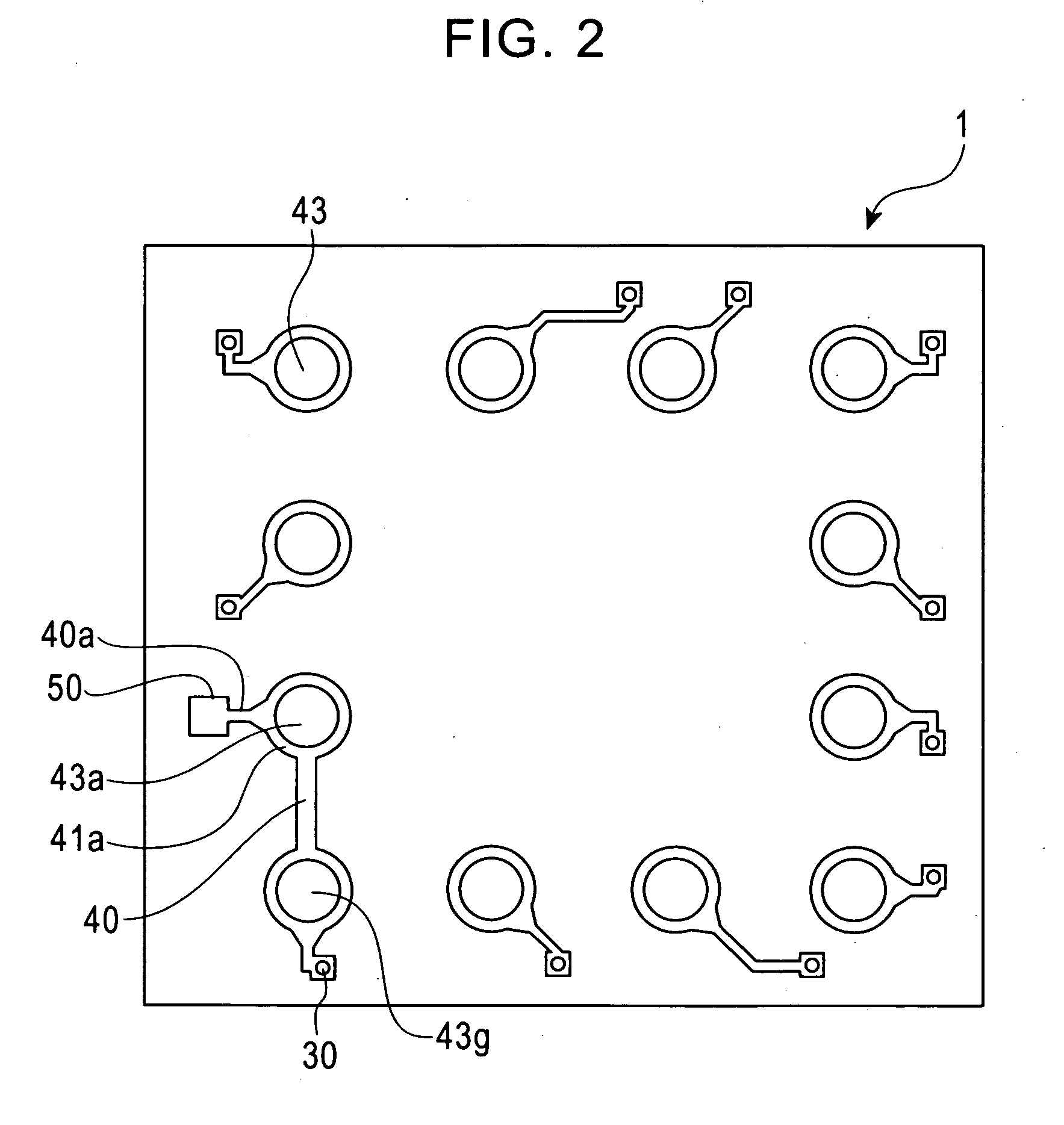
[0070]In the construction shown in FIGS. 1A and 1B, it is possible to apply voltage, different from voltage applied to the external terminal 43 to the potential fixing external terminal 43a, from the voltage application side. The present invention is not limited to this construction, and FIG. 2 shows a modification to this construction. In FIG. 2, voltage applied to the external terminal 43 is used as potential fixing voltage for the silicon substrate layer 11. In a case in which ground potential (GND potential) is used to fix potential of the silicon substrate layer 11, the potential fixing external terminal 43a is connected to an existing GND terminal 43g provided as a functional terminal of the image sensor by a back wire 40. The second embodiment (FIG. 2) is particularly useful when voltage different from voltage applied to the external terminal 43 cannot be applied to the potential fixing external terminal 43a, for example, due to the circumstances of the voltage application si...

third embodiment

[0071]FIGS. 3A and 3B illustrate another modification to the first embodiment. In these drawings, an existing functional terminal is used as the potential fixing external terminal 43a. FIG. 3A is a bottom view illustrating the construction of the image sensor 1, and FIG. 3B is a cross-sectional view. In a case in which ground potential (GND potential) is used to fix potential of the silicon substrate layer 11, an existing GND terminal 43g provided as a functional terminal of the image sensor 1 is used as the potential fixing external terminal 43a, and therefore, it is possible to use ground potential applied to the GND terminal 43g as potential fixing voltage for the silicon substrate layer 11. In this case, a back contact 50 is formed in the vicinity of the GND terminal 43g, and the back contact 50 is connected to the GND terminal 43g (or terminal 43a) by a back wire 40. The third embodiment (FIGS. 3A and 3B) is particularly useful when the potential fixing external terminal 43a ca...


PUM


Abstract

A semiconductor device manufacturing method includes etching a silicon on insulator (SOI) from its surface (i.e., semiconductor substrate layer) to form a first trench and a second trench. The first trench extends through the SOI substrate and reaches an electrode pad. The second trench terminates in the semiconductor substrate layer. The manufacturing method also includes forming an insulation film that covers the surface of the semiconductor substrate layer as well as the side walls and bottoms of the first and second trenches. The manufacturing method also includes removing the insulation film from the bottoms of the first and second trenches to expose the electrode pad from the first trench bottom and to expose the semiconductor substrate layer from the second trench bottom. The manufacturing method also includes forming a conductive film that covers the semiconductor substrate layer and the side walls and the bottoms of the first and second trenches to form a through via electrically connected to the electrode pad at the first trench bottom and to form a contact part electrically connected to the semiconductor substrate layer at the second trench bottom. The manufacturing method also includes patterning the conductive film on the semiconductor substrate layer to form the external electrodes and to form a potential fixing external electrode electrically connected to the contact part.

Description

BACKGROUND OF THE INVENTION[0001]1. Field of the Invention[0002]The present invention relates to a semiconductor device and a manufacturing method thereof, and, more particularly, to a semiconductor device including a silicon on insulator (SOI) device.[0003]2. Description of the Related Art[0004]An SOI device has a silicon substrate layer and a thin film silicon layer (hereinafter, referred to as an SOI layer) provided on the silicon substrate layer. The silicon substrate layer is separated from the thin film silicon layer by a buried oxide film layer (hereinafter, referred to as a BOX layer) in an insulated state. Consequently, it is possible to easily achieve insulative separation between neighboring elements. In addition, no parasitic thyristor is formed via the silicon substrate layer, with the result that it is possible to prevent the occurrence of a latch up phenomenon. When a transistor is mounted in the SOI layer on the BOX layer, it is possible to effectively restrain the o...

Claims


Application Information

Patent Timeline
Patent Type & Authority Applications(United States)
IPC IPC(8): H01L31/02
CPCH01L21/743H01L21/76898H01L23/3114H01L23/481H01L27/14618H01L27/14632H01L2224/05H01L2224/02372H01L2224/05548H01L2224/13H01L2224/13021H01L2224/13024H01L2224/16146H01L2924/0002H01L2924/00H01L2224/0401H01L2924/12032H01L2924/1301H01L2224/02351
Inventor IZUMI, TAKASHI
Owner LAPIS SEMICON CO LTD
Why Eureka
Try Eureka