Configuration of trenched semiconductor power device to reduce masked process

Inactive Publication Date: 2010-05-13
FORCE MOS TECH CO LTD
View PDF1 Cites 13 Cited by
  • Summary
  • Abstract
  • Description
  • Claims
  • Application Information

AI Technical Summary

Benefits of technology

[0008]It is another aspect of this invention to further simplify the manufacturing processes by saving both the body mask and the source mask. The further simplified manufacture processes thus achieve product cost savings and further improve the production yield, the device reliability and performance.
[0009]It is another aspect of this invention that the electrical contacts to the source; the gate; the gate-runner is all implemented with a tungsten contact plug disposed in the contact trenches. A Ti or TiN high conductivity layer is also formed to provide greater contact areas to the source metal and gate pads thus reducing the contact resistance. The electrical contacts are further improved with the contact plug directly contact those regions by extending into the source-body regions, the gate polysilicon, and the body doped region under the source-body contact trenches, thus reliable and high performance electrical contacts are provided.

Problems solved by technology

Conventional technologies for manufacturing semiconductor power devices are continuously challenged to further reduce the manufacturing cost by reducing the number of masks applied in the manufacturing processes.
Furthermore, in attempt to miniaturize the device, the technologies are still faced with a limitation that prevents further increase of the cell density on a limited wafer surface area.
Particularly, the limitations are caused by the wafer areas occupied by planar contacts and device configuration that may induce leakage currents thus leading to a breakdown voltage reduction.
However, as shown in FIG. 1B, the structures have planar contacts and such contacts are not suitable for device shrinkage with the planar contact occupies larger areas.
Furthermore, the manufacturing processes of the device are much more complicate and applying more than four masks.
The production cost is therefore increased when a device is configured according to the disclosures made by Darwish.

Method used


Image

  • Configuration of trenched semiconductor power device to reduce masked process
  • Configuration of trenched semiconductor power device to reduce masked process
  • Configuration of trenched semiconductor power device to reduce masked process

Examples


Embodiment Construction

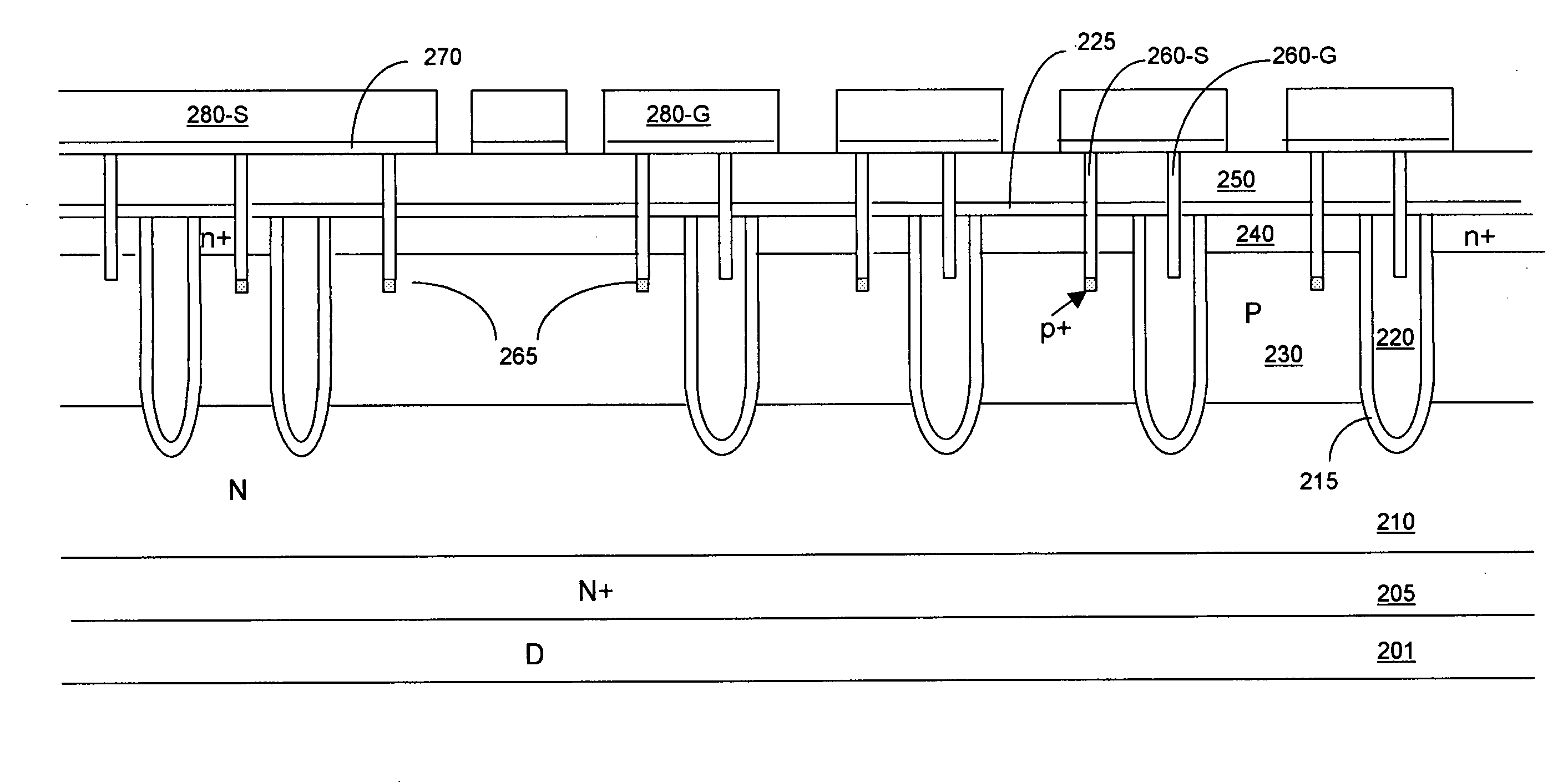
[0017]Please refer to FIGS. 2A and 2B respectively for a side cross sectional view and a top view of an exemplary embodiment of this invention where a metal oxide semiconductor field effect transistor (MOSFET) device 100 is supported on a substrate 105 formed with an epitaxial layer 110. A drain terminal 101 is disposed at the bottom of the substrate 105. The MOSFET device 100 includes a trenched gate 120 disposed in a trench with a gate insulation layer 115 formed over the walls of the trench. A body region 130 that is doped with a dopant of second conductivity type, e.g., P-type dopant, extends between the trenched gates 120. The P-body regions 130 encompassing a source region 140 doped with the dopant of first conductivity, e.g., N+ dopant. The source regions 140 are formed near the top surface of the epitaxial layer surrounding the trenched gates 120. The top surface of the semiconductor substrate extending over the top of the trenched gate, the P body regions 130 and the source...


PUM


Abstract

A semiconductor power device formed on a semiconductor substrate of a first conductivity type wherein the semiconductor power device includes trench gates surrounded by body regions of a second conductivity type encompassing source regions of the first conductivity type therein. The semiconductor power device further includes trench contact structure having a plurality of trench contacts with trenches extended into the body regions for as source-body contacts and extended into the trench gates as gate contact. The semiconductor power device further includes a termination area wherein a plurality of the trench gate contacts are electrically connected to the source-body contacts.

Description

BACKGROUND OF THE INVENTION[0001]1. Field of the Invention[0002]This invention relates generally to the cell structure, device configuration and fabrication process of power semiconductor devices. More particularly, this invention relates to a novel manufacturing processes with reduced masks by implementing improved termination configuration with trench contacts for both gate and source-body regions and multiple trench gates that are connected to the source-body regions in the termination areas thus preventing leakage currents.[0003]2. Description of the Related Art[0004]Conventional technologies for manufacturing semiconductor power devices are continuously challenged to further reduce the manufacturing cost by reducing the number of masks applied in the manufacturing processes. Furthermore, in attempt to miniaturize the device, the technologies are still faced with a limitation that prevents further increase of the cell density on a limited wafer surface area. Particularly, the li...

Claims


Application Information

Patent Timeline
IPC IPC(8): H01L29/78H01L21/336
CPCH01L29/0696H01L29/404H01L29/407H01L29/7813H01L29/4238H01L29/456H01L29/7811H01L29/41766
Inventor HSHIEH, FWA-IUAN
Owner FORCE MOS TECH CO LTD
Why Eureka
Try Eureka