Dual-mode mixer circuit and method

a mixer circuit and dual-mode technology, applied in the field of mixer circuit and frequency transformation method, can solve the problems of increasing testing time and hence costs, direct up-conversion architecture suffers from a so-called lo pulling problem, and still exists direct current offset in direct conversion architectures

Active Publication Date: 2010-05-13
NXP BV
View PDF9 Cites 33 Cited by
  • Summary
  • Abstract
  • Description
  • Claims
  • Application Information

AI Technical Summary

Benefits of technology

[0007]An object of the present invention is to provide a mixer circuit and mixing method, by

Problems solved by technology

However, several problems such as direct current (DC) offset still exist in direct conversion architectures.
To solve these problems main efforts have been put on factory calibration, thus increasing testing time and hence costs.
On the other hand, in digital video broadcast (DVB) receivers there is a demand to reject interferences at 3rd order and 5th order harmonics of the desired carrier frequencies, which interferences are introduced by strong transmission signals of 2nd generation (2G) and 3rd generation (3G) wireless applications and cannot be completely

Method used


Image

  • Dual-mode mixer circuit and method
  • Dual-mode mixer circuit and method
  • Dual-mode mixer circuit and method

Examples


first embodiment

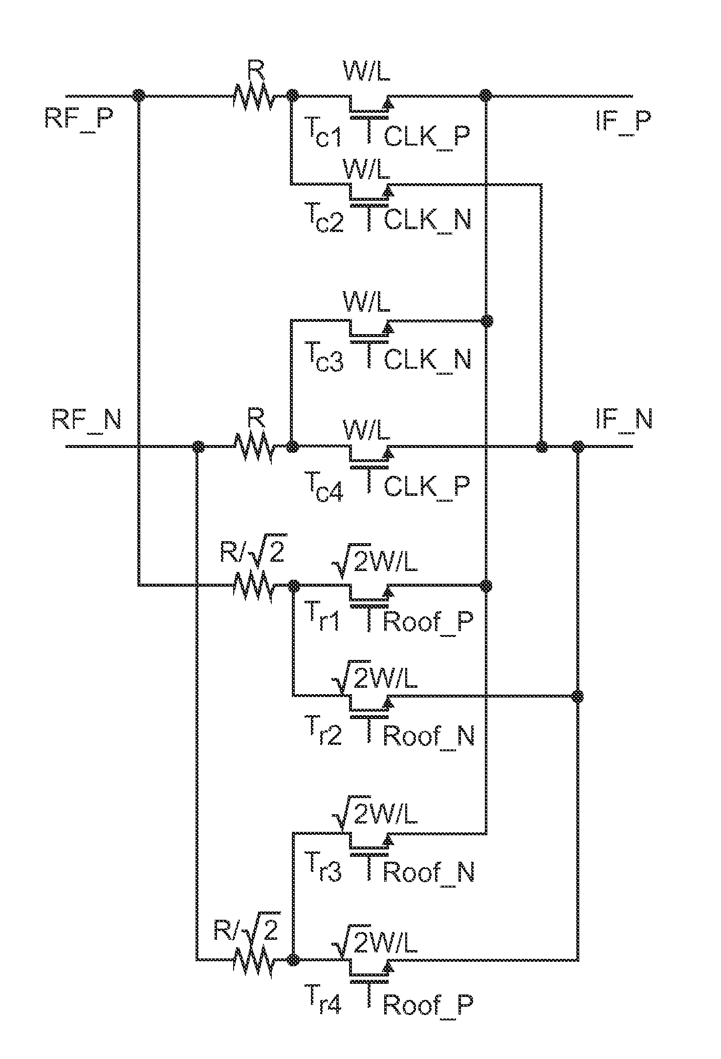
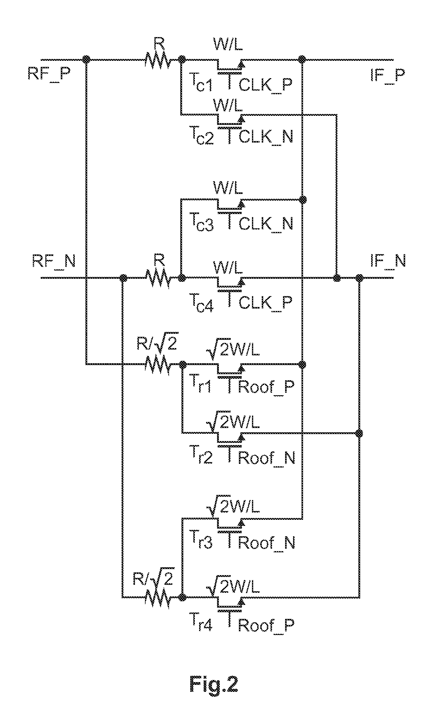
[0032]FIG. 2 shows a schematic circuit diagram of a mixer circuit in a harmonic-rejection mode. This mixer circuit comprises two NMOS (N-channel metal oxide semiconductor) switching cores, wherein the upper switching core comprises transistors Tc1, Tc2, Tc3 and Tc4 which are fed by 50% duty cycle local oscillator signals of positive polarity (CLK_P) and negative polarity (CLK_N), respectively, and a lower switching core which comprises transistors Tr1, Tr2, Tr3 and Tr4 which are fed by 25% duty cycle local oscillator signals of positive polarity (Roof_P) and negative polarity (Roof_N), respectively. By setting the transistor widths in the lower switching core √2 times the transistor widths in the upper switching core, and the resistance in the lower switching core 1 / √2 times the resistance in the upper switching core, the current yielded in the bottom switching core is √2 times the current yielded in the upper switching core when they are both switched on. Due to the current summin...

second embodiment

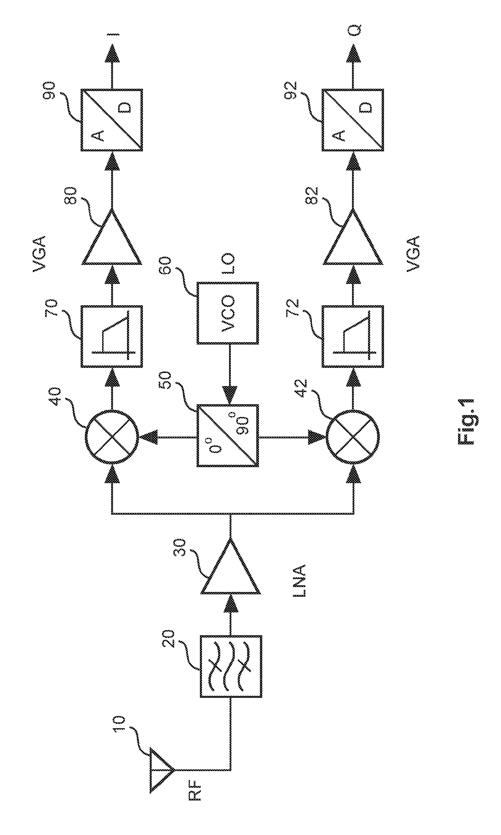
[0034]FIG. 4 shows a schematic block diagram of a direct conversion transmitter according to a Similar to the above direct conversion receiver architecture, direct up-conversion is introduced in many applications for transmitter architectures, due to its high level integration option. As shown in FIG. 4, the LO frequency is equal to the carrier frequency, thus eliminating any intermediate up-conversion employed in a dual up-conversion architecture. Therefore, the image problem is no longer present and a high quality factor discrete RF filter in front of a PA 220 can be avoided. In the transmitter architecture of FIG. 4, baseband I and Q components are supplied to respective mixer circuits 240, 242 to which an in-phase component and a quadrature component of a local oscillator signal generated by a VCO 260 is applied. The required phase shift is obtained by a phase shifting circuit 250. Both mixer output signals are summed by an adder circuit 230 and supplied to the PA 220 in order ...

third embodiment

[0042]FIG. 9 shows a schematic circuit diagram of a mixer circuit which can be applied as the mixer circuit 340 of FIG. 8, according to a Additionally, FIG. 9 shows waveforms of the local oscillation signal fVCO generated by the VCO 310 and phase signals f0(t), f1(t), f2(t) and f3(t) to be supplied via the waveform combiner 330 to the mixer circuit 340. Each of four mixers provided in the mixer circuit 340 to translate or transform the frequency of a desired signal from baseband to IF is realized with three active current-commuting sub-mixers all feeding common resistive loads connected to a voltage supply line Vdd, as shown in FIG. 9.

[0043]Each of the three sub-mixers of FIG. 9 receives the same baseband input BB through scaled input devices. However, the switches in each sub-mixer are driven by respective ones of the four phase components generated by the divide-by-four circuit 320 based on the local oscillator signal. Each sub-mixer generates a typical square wave response with ...


PUM


Abstract

The present invention relates to a mixer circuit and method of frequency transformation, wherein an input signal is switched in accordance with a first local oscillator signal and in accordance with at least one second local oscillator signal having a smaller duty cycle than said first local oscillator signal, or having a respective predetermined phase shift with respect to said first local oscillator signal. Output signals obtained by the switching in accordance with the first and at least one second local oscillator signals are summed and the polarity of one of said first local oscillator signal and said at least one second local oscillator signal is switched in response to a control input, to thereby switch between a harmonic-rejection mode and a sub-harmonic mixing mode.

Description

FIELD OF THE INVENTION[0001]The present invention relates to a mixer circuit and method of frequency transformation, which can be used for example in transceiver, transmitter or receiver applications of wireless systems.BACKGROUND OF THE INVENTION[0002]Increasing demand for transceiver devices with small form factors has motivated research on highly integrated low-cost transmitter and receiver circuits. Direct conversion transmitter and receiver circuits can simplify the signal path by translating a desired radio frequency (RF) spectrum to a zero intermediate frequency (IF) via a single mixing stage or circuit, and thus effectively eliminate image frequency problems and hence expensive and bulky off-chip image-reject filters required in conventional heterodyne receivers. It also allows for channel selection to be performed at baseband with a simple low-pass filtering prior to a high dynamic analog-to-digital conversion. Therefore, the direct conversion approach can offer highly inte...

Claims


Application Information

Patent Timeline
IPC IPC(8): H04B1/40G06G7/14H04B1/04H03D7/16
CPCH03D7/1441H03D7/166H03D2200/0086H03D2200/0084H03D7/1466H03D7/1483H03D7/1458
Inventor HE, XIN
Owner NXP BV
Why Eureka
Try Eureka