[0006]The AuSn paste is a bonding material paste containing a powdered solder in a ball shape, organic solvents and flux, and has a
melting point of 280° C. The powdered solder includes an
alloy of Au (content: 70 to 75%) and
tin (content: 17 to 22%). The flux is used for removing the
surface oxide film formed on the bonded surfaces, preventing the re-oxidization of solder when bonding, reducing the
surface tension of molten solder, and the like. The flux is mainly composed of
rosin (C19H29COOH, content: 3 to 6%). The
organic solvent is used for dissolving the
solid components and imparting an appropriate
viscosity to the material. The
organic solvent may contain, for example,
diethylene glycol monohexyl
ether (C6H13(OCH2CH2)2OH, content: 1 to 2%,
boiling point: 259° C.), and 2-ethyl-1,3-
hexane diol (C3H7CH(OH)CH(C2H5)CH2OH, content: 2% or less,
boiling point: 244° C.).
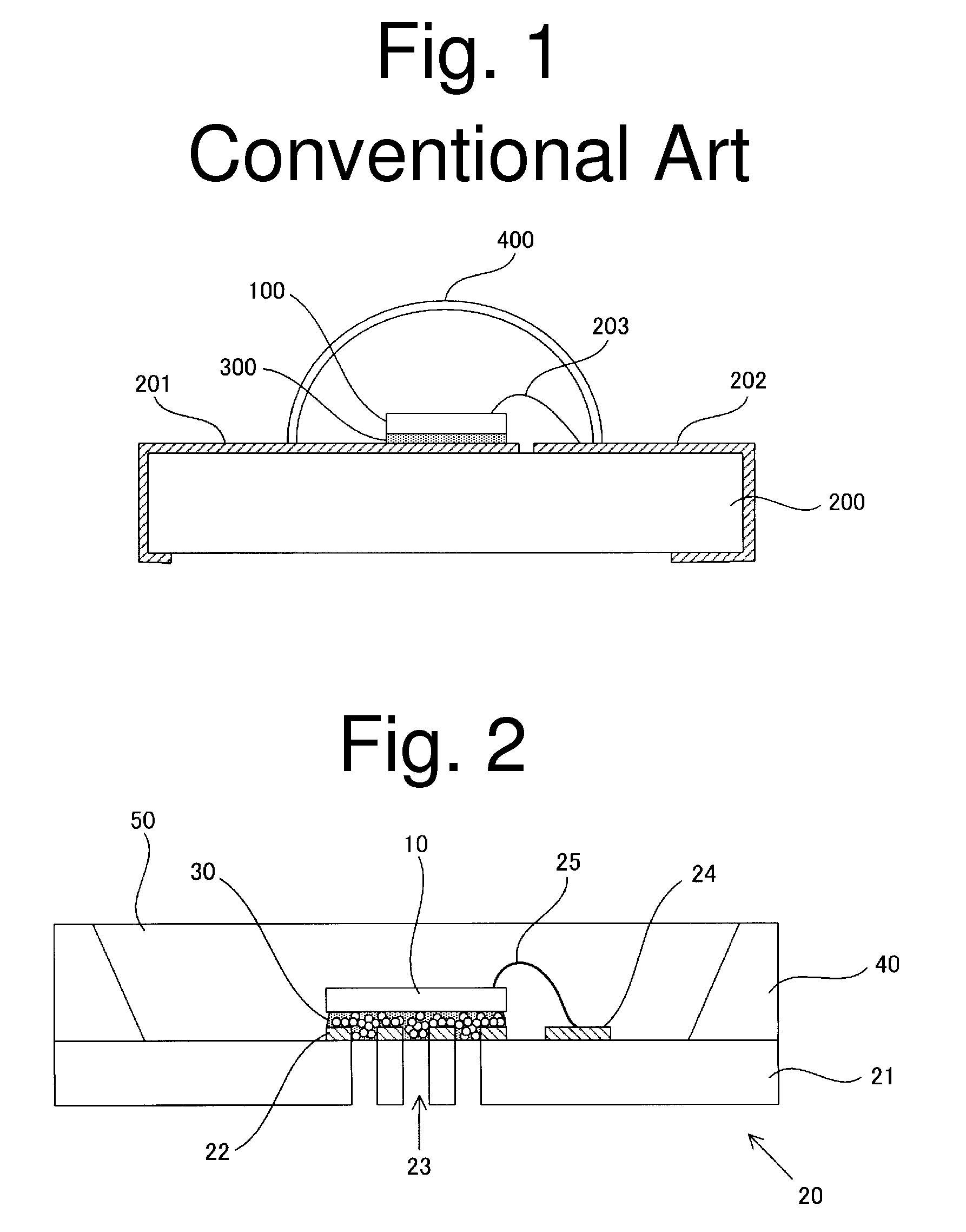
[0007]When an optical semiconductor element is bonded to a die pad of a package substrate using an AuSn paste, the AuSn paste is applied onto the die pad. Then, the optical semiconductor element is mounted on the die pad, and the reflow treatment is performed. The die pad can have a flat surface, and accordingly, the die pad can be in
close contact with the optical semiconductor element with the AuSn paste interposed therebetween. In this state, they are transferred into a reflow furnace. Here, the
boiling point of the
solvent contained in the AuSn paste is lower than the
melting point of AuSn as shown in Table 1. In this case, if a pre-heating step is eliminated or the pre-heating is not sufficient in the reflow treatment, the
solvent contained therein cannot sufficiently evaporate in advance. Namely, the
environmental temperature reaches the boiling point of the solvent while the solvent is still contained in the paste. In this case, i.e., when the increasing temperature in the reflow treatment reaches the
melting temperature, the solvent may abruptly boil before AuSn melts. As the optical semiconductor element and the die pad are in
close contact with each other, there may be no path for discharging the gasified solvent. In this case, a so-called “
chip fly” event may occur wherein the pressure of the gasified solvent blows the optical semiconductor element that is mounted on the die pad off. In order to solve or prevent this problem, pre-heating treatment can be done in a sufficient amount for the solvent to evaporate. Namely, the reflow treatment step can include a temperature profile setting for
temperature control in which temperatures lower than the boiling point of the solvent being used are maintained for a predetermined time before reaching the
melting temperature of AuSn, resulting in increased total time for reflow treatment.
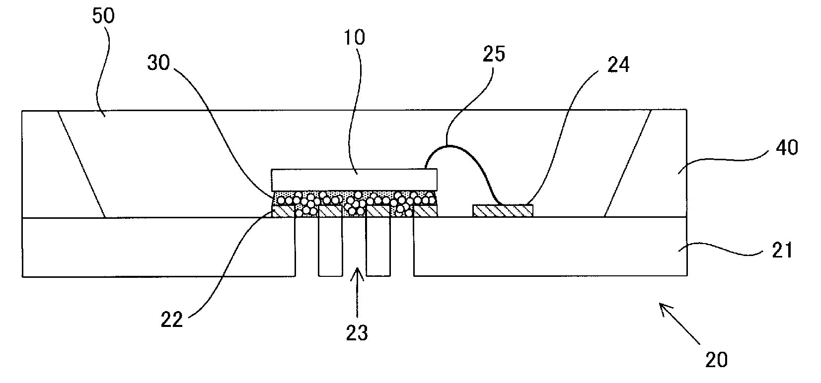
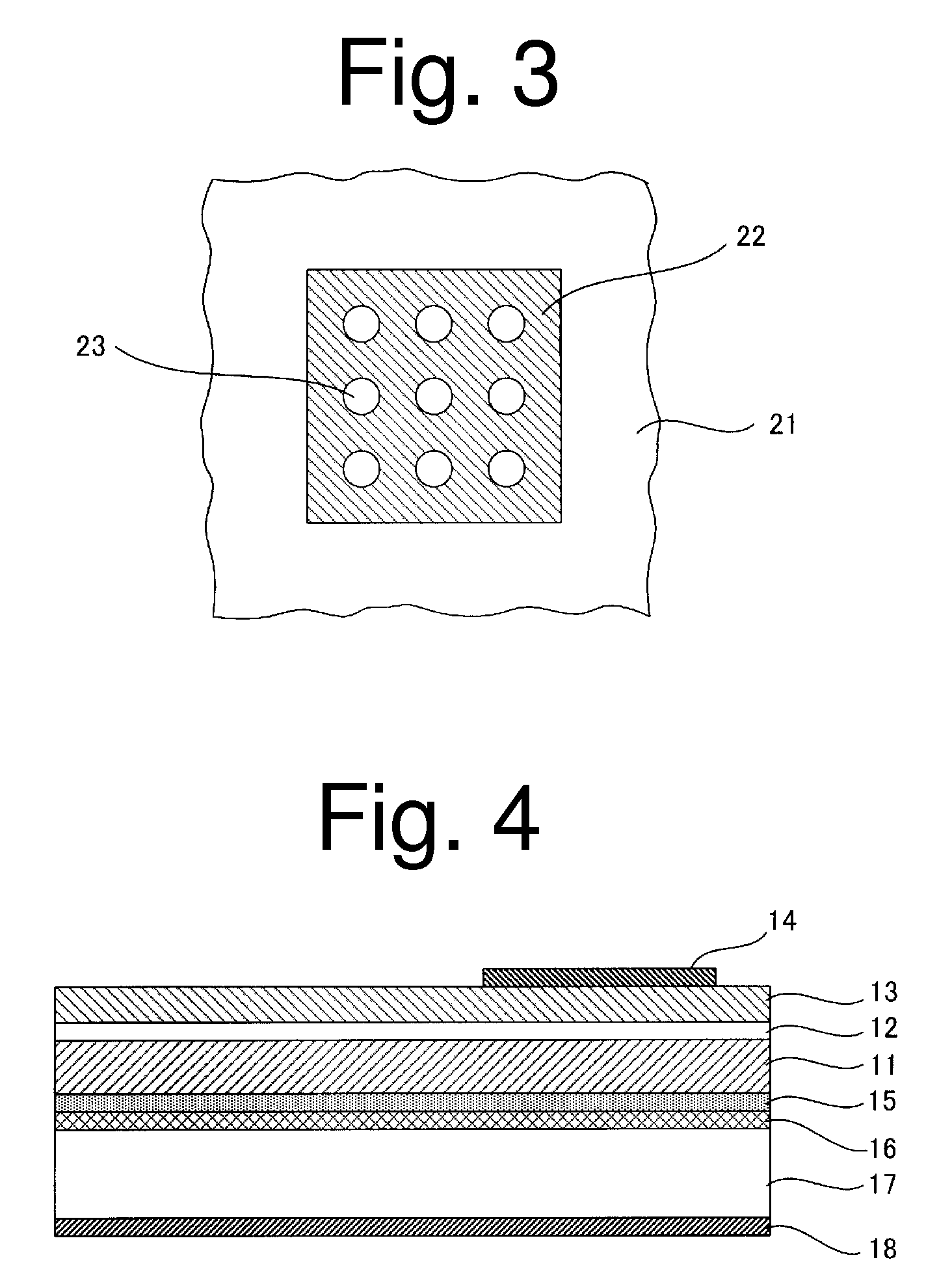
[0013]An exemplary optical semiconductor apparatus made in accordance with principles of the presently
subject matter can have a plurality of through holes penetrating both the
ceramic base material and the die pad constituting the substrate. These through holes can function as the discharging paths for gases generated by evaporating solvent contained in the
solder paste in the reflow treatment step. Accordingly, the problems associated with
chip fly due to the abrupt gas generation can be almost completely solved. This can allow for the
elimination of the pre-heating treatment in the reflow treatment step, resulting in significant reduction of reflow
treatment time.

