Semiconductor device and manufacturing method thereof

a technology of semiconductor devices and manufacturing methods, applied in semiconductor devices, semiconductor/solid-state device details, electrical apparatus, etc., can solve problems such as difficulty in achieving effective dielectric constants, and achieve the effects of reducing capacitance variations, increasing capacitance variations, and reducing capacitance variations

Active Publication Date: 2010-05-27
KOKUSA ELECTRIC CO LTD
View PDF20 Cites 254 Cited by
  • Summary
  • Abstract
  • Description
  • Claims
  • Application Information

AI Technical Summary

Benefits of technology

[0006]Patent Document 1 shows that the capacitance is reduced by adopting an air-gap structure, compared with a normal Damascene structure. However, according to the studies by the inventor, in a conventional structure depicted in (a) of FIG. 1 where a barrier insulating film is present on the bottom of an air gap, it is difficult to achieve an effective dielectric constant presented in International Technology Roadmap for Semiconductors (ITRS) in the next generation of 32 nm nodes onward. By contrast, according to the studies by the inventor, in a structure according to the present invention depicted in (b) of FIG. 1, that is, in a structure where no barrier insulating film is present on the bottom of the air gap, a capacitance reduction effect of approximately 12% to 13% is obtained by removing just a slight barrier insulating film, so that an effective dielectric constant desired for 32 nm nodes onward can be achieved.
[0007]Patent Document 2 discloses an example where an inter-wiring insulating film is formed deeper than the bottom of a trench. In Patent Document 2, however, no consideration is given to the measures for reducing capacitance variations. Depth variations become more conspicuous as the etching becomes deeper, and it causes an increase in capacitance variations. In the present invention, a through-hole interlayer insulating film made of a material different from that of the inter-wiring insulating film is formed at a depth-direction position in which the air gap is desired to be formed, and etching for the removal of the inter-wiring insulating film is stopped by a via interlayer insulating film. By this means, the capacitance variations can be more reduced compared with the conventional structure.
[0008]An object of the present invention is to provide a semiconductor device capable of reducing capacitance between wirings having a main conductive layer made of copper, and a manufacturing method of the semiconductor device.

Problems solved by technology

However, the result of studies by the inventor has found that the following problems arise in the above-mentioned buried wiring technique using copper as a main conductive layer.
However, according to the studies by the inventor, in a conventional structure depicted in (a) of FIG. 1 where a barrier insulating film is present on the bottom of an air gap, it is difficult to achieve an effective dielectric constant presented in International Technology Roadmap for Semiconductors (ITRS) in the next generation of 32 nm nodes onward.

Method used


Image

  • Semiconductor device and manufacturing method thereof
  • Semiconductor device and manufacturing method thereof
  • Semiconductor device and manufacturing method thereof

Examples


first embodiment

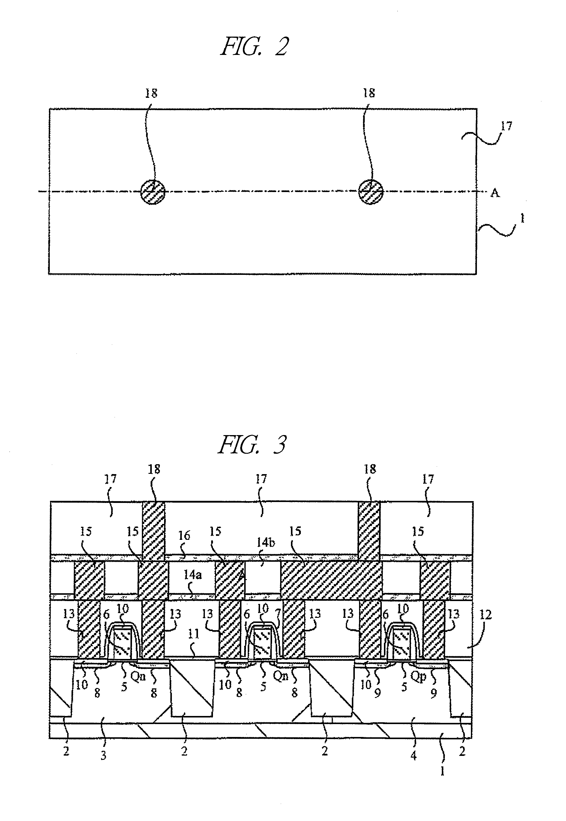
[0089]A semiconductor device and a manufacturing method thereof according to a first embodiment will be described with reference to the drawings. FIG. 2 is a plan view of principal parts in the manufacturing process of a semiconductor device, for example, Complementary Metal Insulator Semiconductor Field Effect Transistor (CMISFET) according to an embodiment of the present invention. FIG. 3 is a cross-sectional view of an A-A line in FIG. 2. As depicted in FIGS. 2 and 3, a wafer or semiconductor substrate 1 made of p-type monocrystalline silicon having a resistivity of, for example, 1 Ωcm to 10 Ωcm has isolation regions 2 formed on its main surface. The isolation regions 2 are made of silicon oxide or the like and are formed by, for example, Shallow Trench Isolation (STI) or LOCOS (Local Oxidization of Silicon).

[0090]The semiconductor substrate 1 has a p-type well 3 and an n-type well 4 formed from its main surface to a predetermined depth. The p-type well 3 is formed by, for exampl...

second embodiment

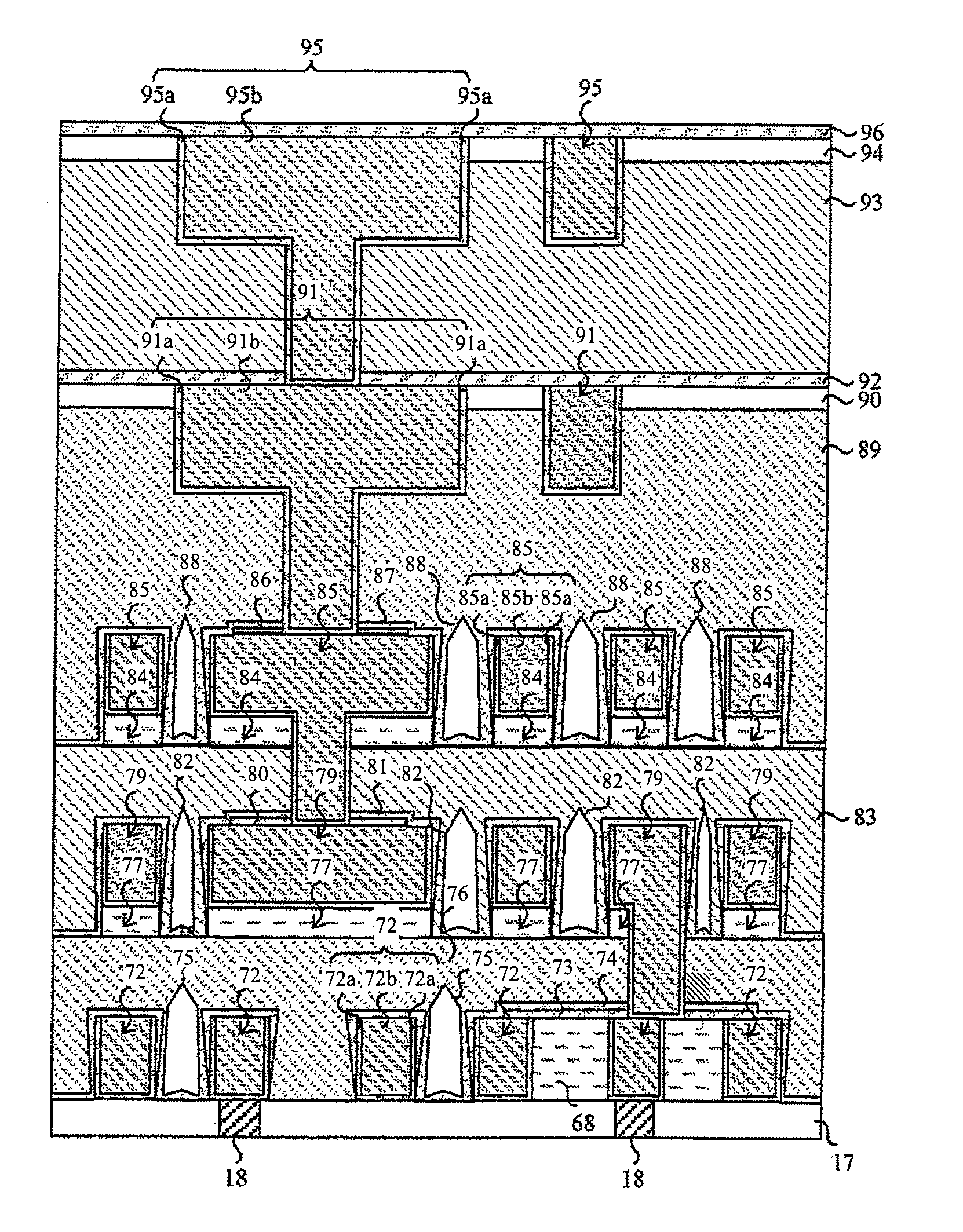
[0143]FIG. 32 is a cross-sectional view of principal parts in the manufacturing process of a semiconductor device according to a second embodiment of the present invention. The semiconductor device of the present embodiment has a multilayer wiring structure where the structure having a wiring layer and a reservoir in which air gaps are formed between adjacent wirings and these adjacent wirings are not connected via a CMP surface like the second layer wirings 26 and the third layer wirings 47 of the first embodiment and a wiring layer formed by using a general buried wiring technique are combined. In FIG. 31, up to the process of forming an insulating film 60 on an upper portion of fourth layer wirings 55, the manufacturing process is almost similar to those described with reference to FIGS. 4 to 10 and FIGS. 18 to 30 of the first embodiment, and therefore, the description thereof is omitted and the subsequent manufacturing process will be described here.

[0144]Fifth and subsequent wi...

third embodiment

[0147]FIG. 33 is a cross-sectional view of principal parts in the manufacturing process of a semiconductor device according to a third embodiment of the present invention continued from FIG. 3. Also in FIG. 33, the illustration of portions corresponding to the structure below the insulating film 17 in FIG. 3 is omitted.

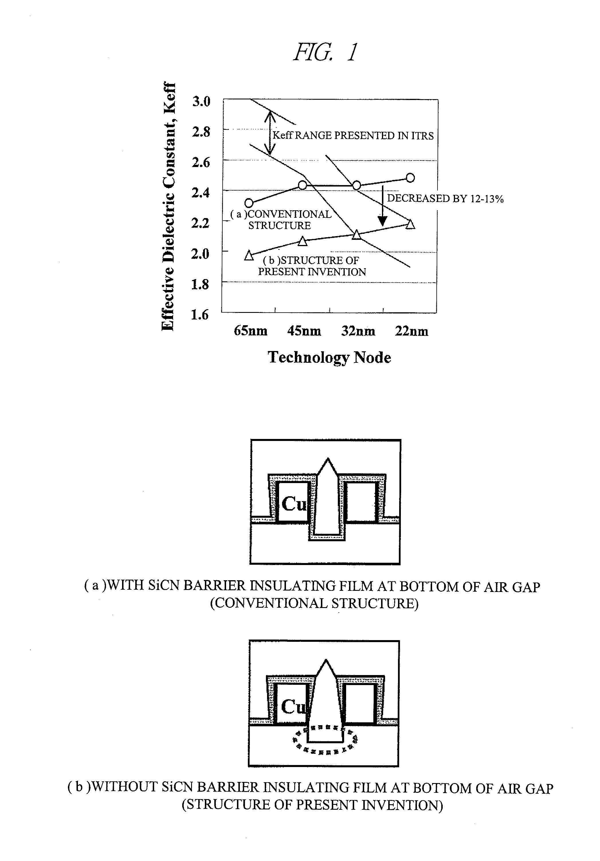
[0148]The present embodiment discloses air-gap wirings whose capacitance variations are more reduced than those of the air-gap wirings described in the first embodiment by using a via interlayer insulating film made of a material different from a wiring interlayer insulating film as an etching stopper.

[0149]FIGS. 33 to 35 are cross-sectional views of principal parts in the manufacturing process of a semiconductor device continued from FIG. 2.

[0150]First, in the present embodiment, as depicted in FIG. 33A, an insulating film 67 is formed on the insulating film 17 having the through holes 18 embedded therein. For the insulating film 67, a Low-K material or an insulating...


PUM

PropertyMeasurementUnit
resistivityaaaaaaaaaa
dielectric constantaaaaaaaaaa
voltageaaaaaaaaaa

Abstract

Wirings mainly containing copper are formed on an insulating film on a substrate. Then, after forming insulating films for reservoir pattern and a barrier insulating film, an insulating film for suppressing or preventing diffusion of copper is formed on upper and side surfaces of the wirings, the insulating film on the substrate, and the barrier insulating film. Here, thickness of the insulating film for suppressing or preventing diffusion of copper at the bottom of a narrow inter-wiring space is made smaller than that on the wirings, thereby efficiently reducing wiring capacitance of narrow-line pitches. Then, first and second low dielectric constant insulating films are formed. Here, a deposition rate of the first insulating film at an upper portion of the side surfaces of facing wirings is made higher than that at a lower portion thereof, thereby forming air gaps. Finally, the second insulating film is planarized by interlayer CMP.

Description

CROSS-REFERENCE TO RELATED APPLICATION[0001]The present application claims priority from Japanese Patent Application No. JP 2008-276235 filed on Oct. 28, 2008, the content of which is hereby incorporated by reference into this application.TECHNICAL FIELD OF THE INVENTION[0002]The present invention relates to a semiconductor device and a manufacturing technique thereof, and in particular to a technique effectively applied to a semiconductor device having wirings including a main conductive film containing copper as a main component.BACKGROUND OF THE INVENTION[0003]The buried wiring structure is formed by burying a wiring material in a wiring opening such as a wiring trench or hole formed in an insulating film with a wiring formation technique referred to as Damascene technique (Single-Damascene technique and Dual-Damascene technique). However, when a material of the main wiring is copper (Cu), Cu tends to be diffused into an insulating film compared with a metal such as aluminum (Al)...

Claims


Application Information

Patent Timeline
Patent Type & Authority Applications(United States)
IPC IPC(8): H01L21/768
CPCH01L21/76811H01L21/7682H01L21/76834H01L21/76835H01L23/5222H01L2924/0002H01L23/53295H01L21/02697H01L2924/00
Inventor NOGUCHI, JUNJI
Owner KOKUSA ELECTRIC CO LTD
Why Eureka
Try Eureka