Environmental barrier coating for organic semiconductor devices and methods thereof

a technology of organic semiconductor devices and environmental barrier layers, applied in the field of environmental barrier films, can solve the problems of limiting the shelf life and operational stability of many organic electronics devices, affecting the stability of organic semiconductor devices, and cells being subjected to a variety of uncontrollable conditions, so as to reduce the exposure of different primary and secondary barrier layers

Inactive Publication Date: 2010-06-03
GEORGIA TECH RES CORP
View PDF6 Cites 105 Cited by
  • Summary
  • Abstract
  • Description
  • Claims
  • Application Information

AI Technical Summary

Benefits of technology

[0030]To make a sandwich structure, where the organic component is an organic substrate, the method can further include disposing an organic semiconductor device on the passivation layer, followed by disposing a different non-conformal primary barrier layer on the organic semiconductor device, disposing a different conformal secondary barrier layer on the different primary barrier layer by atomic layer deposition, and disposing a different passivation layer on the different secondary barrier layer, wherein the different passivation layer reduces exposure of the different primary and different secondary barrier layers to moisture and oxygen.

Problems solved by technology

Organic semiconductor devices can experience significant degradation from exposure to environmental conditions.
Specifically, oxygen and water vapor are known to cause corrosion or other degradation due to photo-oxidation, which can severely limit the shelf-life and operational stability of many organic electronics devices (e.g., photovoltaic cells, light-emitting diodes, displays, field-effect transistors, and like devices made from organic materials).
Such cells will be subjected to a variety of uncontrollable conditions when deployed in actual, real world applications.
Packaging technologies that have been developed for inorganic optoelectronic materials cannot be applied directly to organic-based materials because they often involve processing temperatures that are too high for organic materials and that would damage the organic layers during the fabrication process.
This packaging approach, however, adds weight and rigidity, thereby precluding use of a device packaged as such in applications that require flexibility of the device.
However, these films are prone to defects, which facilitate the permeation of water vapor and oxygen, resulting in poor protection.
With this approach, however, multiple bilayers (i.e., of the inorganic / organic films) are needed, leading to an increase in the complexity of processing these barrier films.
While ALD-deposited films allow for higher quality inorganic films with fewer defects than seen in PECVD or sputtering, ALD suffers from slow deposition rates, which results in increased deposition times.

Method used


Image

  • Environmental barrier coating for organic semiconductor devices and methods thereof
  • Environmental barrier coating for organic semiconductor devices and methods thereof
  • Environmental barrier coating for organic semiconductor devices and methods thereof

Examples


example 1

Preparation of Environmental Barrier Coatings on Glass Substrates

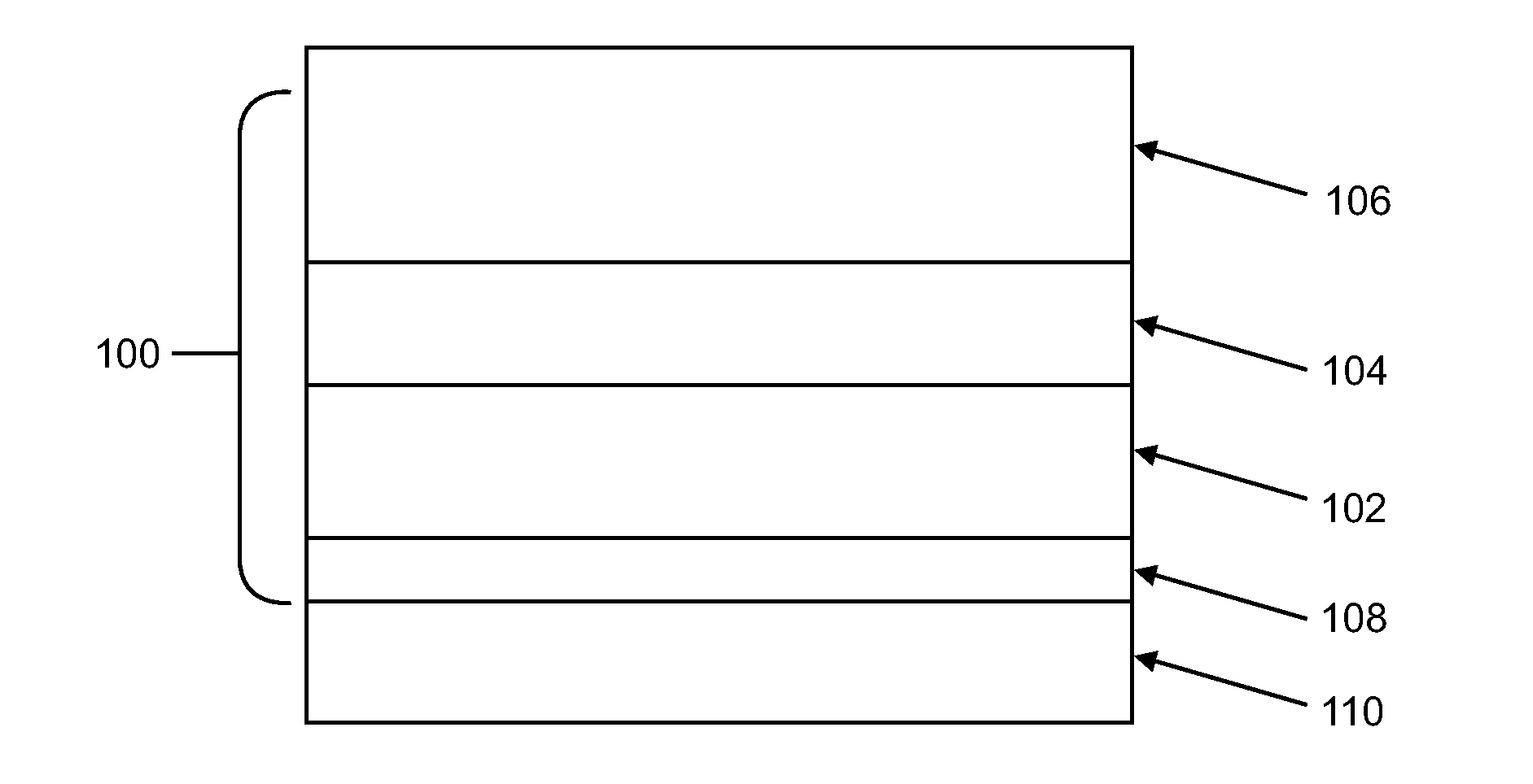
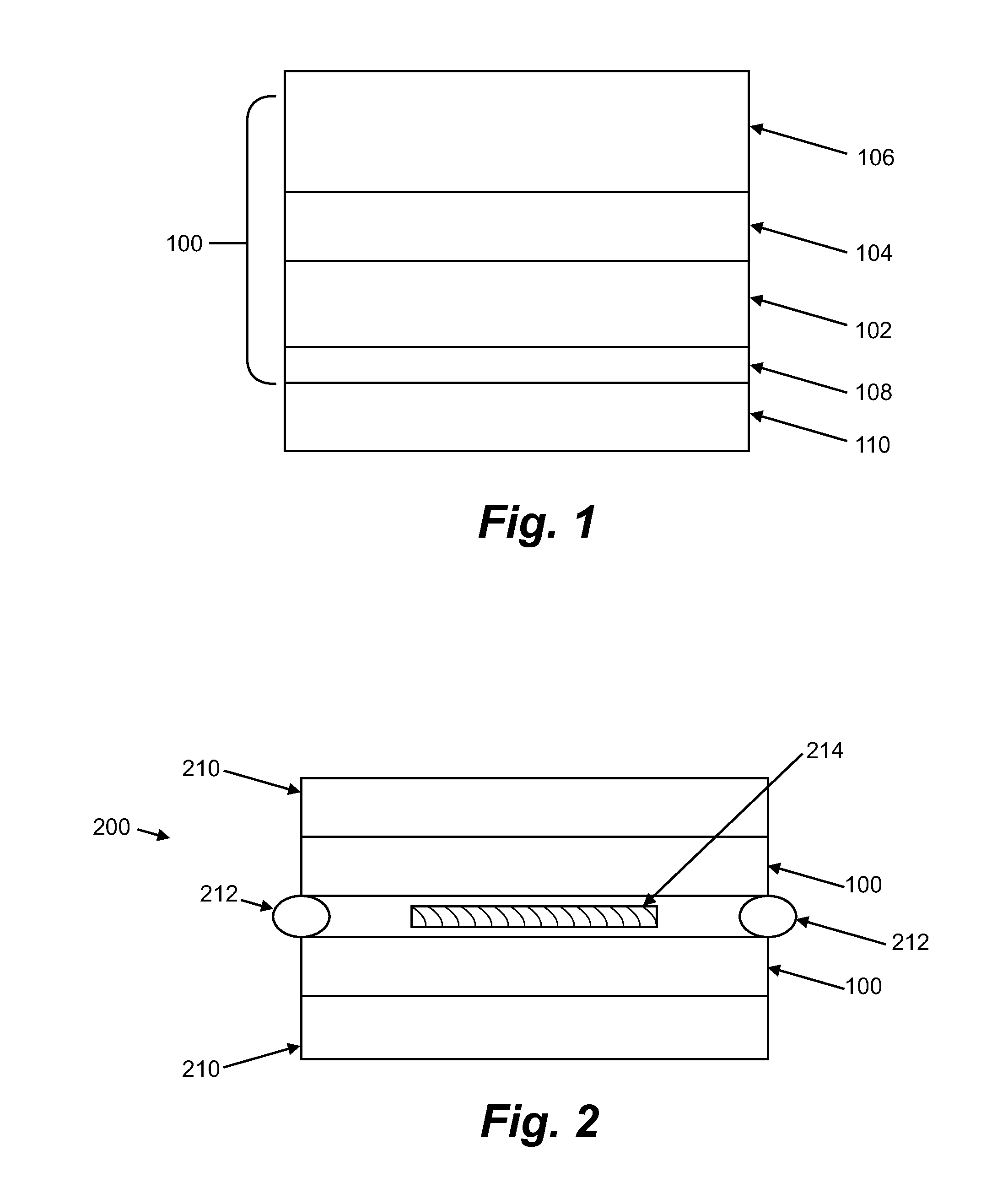
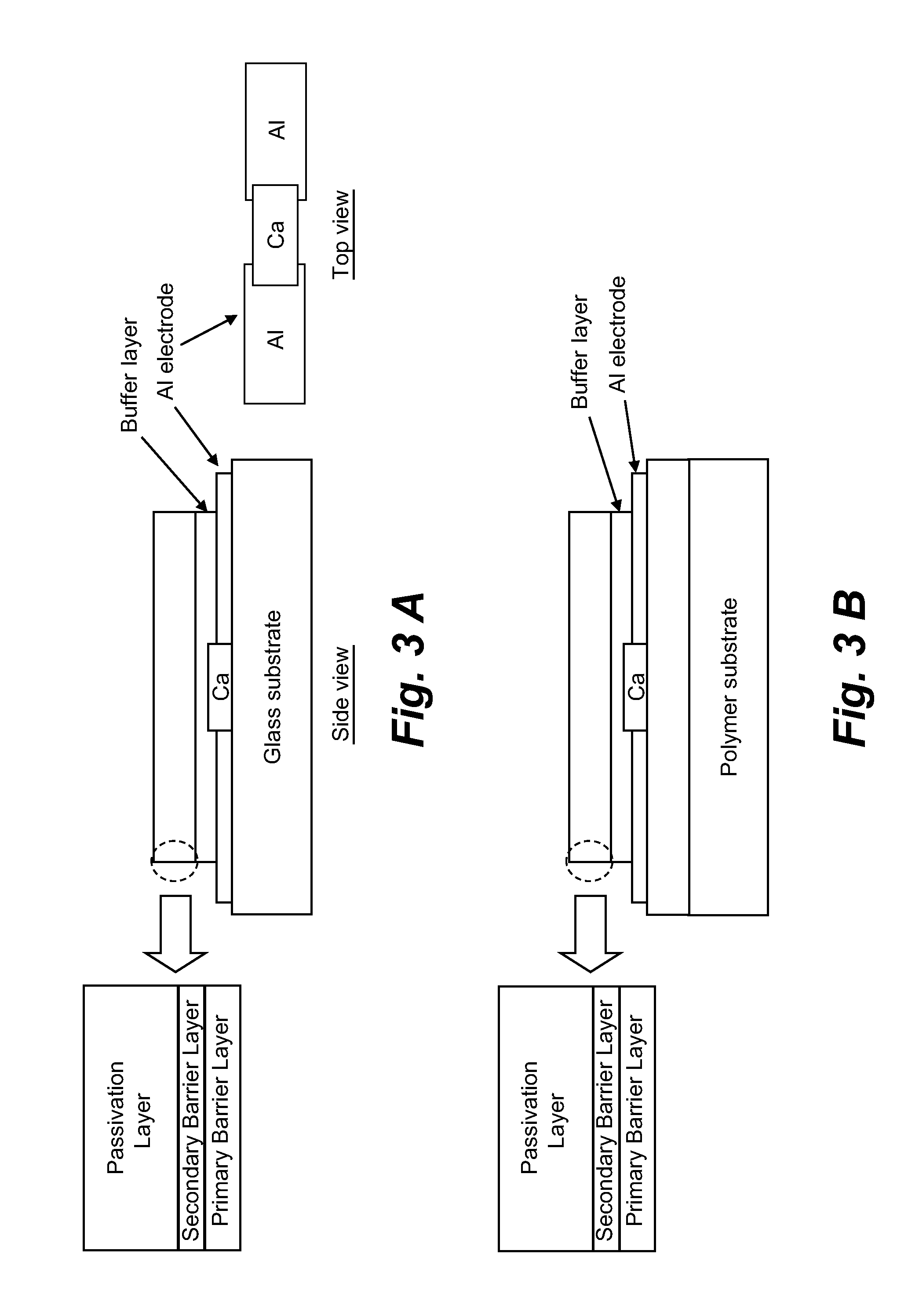
[0100]In this example, the substrate was glass, and a buffer layer comprised of an about 400 nm thick layer of SiOx was deposited on the calcium sensor and two aluminum electrodes using PECVD. A primary barrier layer of SiOx with a thickness of about 100 nm was deposited on the buffer layer using PEVCD. A secondary barrier layer of Al2O3, having a thickness of about 50 nm, was deposited on top of the primary barrier layer using ALD. Finally, a passivation layer of parylene with a thickness of 1 μm was deposited on top of the secondary barrier layer. The complete structure is shown in the FIG. 4A.

[0101]The precursors used for the PECVD depositions included SiH4, N2O, and NH3. The flow rates of SiH4, and N2O were about 400 standard cubic centimeters per minute (sccm) and about 3000 sccm, respectively. The precursors were then reacted between two parallel plates in a radio frequency (RF) induced plasma to deposit SiOx. Th...

example 2

Preparation of Environmental Barrier Coatings on Glass Substrates

[0105]In this example, the substrate was glass, and a buffer layer comprised of an about 400 nm thick layer of SiOx was deposited on the calcium sensor and two aluminum electrodes using PECVD. A primary barrier layer of SiNx with a thickness of about 100 nm was deposited on the buffer layer using PEVCD. A secondary barrier layer of Al2O3, having a thickness of about 50 nm, was deposited on top of the primary barrier layer using ALD. Finally, a passivation layer of parylene with a thickness of 1 μm was deposited on top of the secondary barrier layer. The complete structure is shown in the FIG. 5A.

[0106]The precursors used for the PECVD depositions of SiOx included SiH4, N2O, and NH3. The flow rates of SiH4, and N2O were about 400 sccm and about 3000 sccm, respectively. The precursors used for the PECVD depositions of SiNx included SiH4, N2, He, and NH3. The flow rates of SiH4, N2, He, and NH3 were about 200 sccm, about ...

example 3

Preparation of Environmental Barrier Coatings on Glass Substrates

[0110]In this example, a device was prepared exactly as described in Example 1, with the exception that the secondary barrier layer of Al2O3, grown using ALD, was prepared with a thickness of about 10 nm. A schematic illustration of this structure is shown in FIG. 6A.

[0111]As shown in FIG. 6B, where the circles represent experimental data and the lines were fitted to extract effective WVTR values, the change in electrical conductance measured as a function of time yielded an effective WVTR value of about 4±0.5×10⁻⁵ g / m2 / day.


PUM

PropertyMeasurementUnit
thicknessaaaaaaaaaa
thicknessaaaaaaaaaa
thicknessaaaaaaaaaa

Abstract

Improved environmental barrier coatings and improved organic semiconductor devices employing the improved environmental barrier coatings are disclosed herein. Methods of making and using the improved coatings and devices are also described. An improved environmental barrier coating generally includes a primary barrier layer, a secondary barrier layer disposed on the primary barrier layer, and a passivation layer disposed on the secondary barrier layer. The secondary barrier layer is formed using atomic layer deposition.

Description

CROSS-REFERENCE TO RELATED APPLICATION[0001]The present application claims the benefit of U.S. Provisional Patent Application No. 61 / 119,200, filed 2 Dec. 2008, and entitled “Environmental Barrier Coating for Organic Semiconductor Devices and Method Thereof”, which is hereby incorporated by reference in its entirety as if fully set forth below.STATEMENT OF FEDERALLY SPONSORED RESEARCH[0002]This invention was made with United States Government support under agreement number DMR-0120967 awarded by the National Science Foundation. The United States Government has certain rights in this invention.TECHNICAL FIELD[0003]The various embodiments of the present invention relate generally to improved organic devices and their associated fabrication processes, and more particularly to improved environmental barrier films and to methods for making such films.BACKGROUND[0004]Organic semiconductor devices can experience significant degradation from exposure to environmental conditions. Specificall...

Claims


Application Information

Patent Timeline
Patent Type & Authority Applications(United States)
IPC IPC(8): H01L31/042B32B9/04B32B27/32B32B27/38B32B27/30B32B27/00B32B27/40B32B5/00H01L31/04C23C16/44C23C16/513H01J1/62H01L51/50H01L51/56H01L51/05
CPCC23C16/0272C23C16/403Y10T428/26C23C16/56H01L51/5237C23C16/45525Y10T428/31663Y10T428/31504Y10T428/31551Y10T428/31935Y10T428/31721Y10T428/31938Y10T428/31511H10K50/844
Inventor GRAHAM, JR., SAMUELKIPPELEN, BERNARDKIM, NAMSUDOMERCQ, BENOIT
Owner GEORGIA TECH RES CORP
Why Eureka
Try Eureka