Encapsulant material, crystalline silicon photovoltaic module and thin film photovoltaic module

a technology of crystalline silicon and photovoltaic modules, applied in the direction of pv power plants, other domestic articles, synthetic resin layered products, etc., can solve the problems of unfavorable applications of above-ground methods in see-through type thin film photovoltaic modules, and achieve the effect of improving light trapping and encapsulating light reflection

Active Publication Date: 2010-06-17
IND TECH RES INST
View PDF8 Cites 69 Cited by
  • Summary
  • Abstract
  • Description
  • Claims
  • Application Information

AI Technical Summary

Benefits of technology

[0011]Therefore, the present invention provides a novel structure of an encapsulant material for a photovoltaic module, which has porous structure of several hundreds of nanometers to several hundreds of micrometers to enhance light reflectivity inside the encapsulant, so as to improve the light trapping of, for example 1) crystalline silicon photovoltaic module and 2) thin film photovoltaic module.

Problems solved by technology

However, the above method is unfavorable for applications in see-through type thin film photovoltaic module.

Method used


Image

  • Encapsulant material, crystalline silicon photovoltaic module and thin film photovoltaic module
  • Encapsulant material, crystalline silicon photovoltaic module and thin film photovoltaic module
  • Encapsulant material, crystalline silicon photovoltaic module and thin film photovoltaic module

Examples


first embodiment

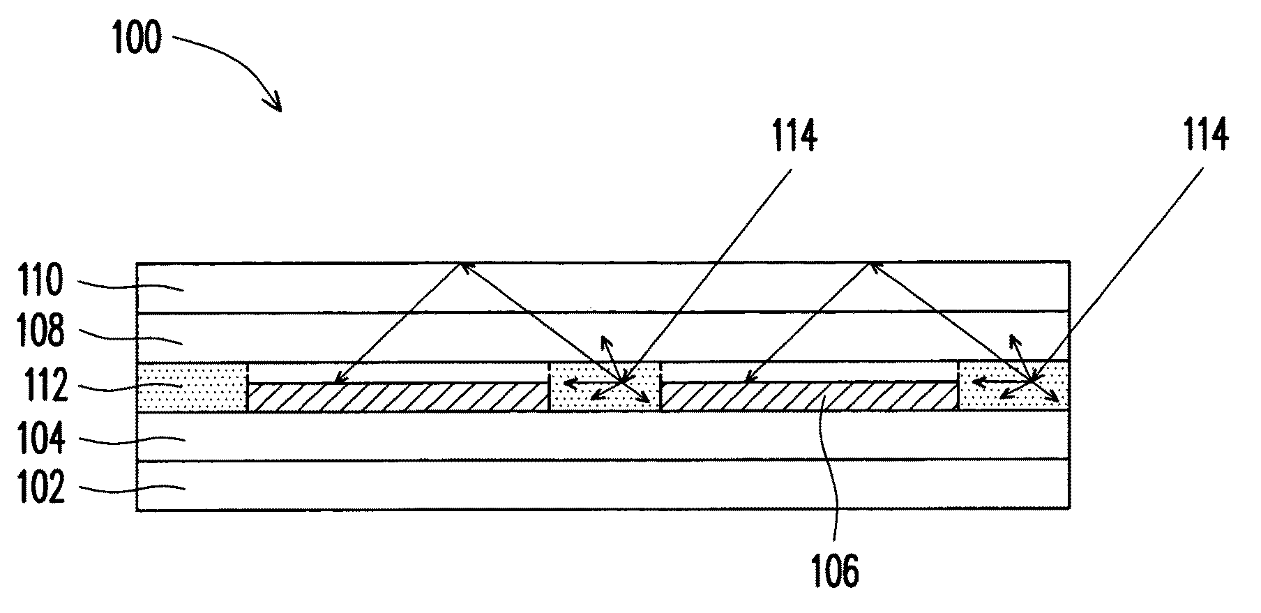
[0049]FIG. 1 is a schematic cross-sectional view showing a crystalline silicon photovoltaic module according to the first embodiment of the present invention.

[0050]Referring to FIG. 1, a crystalline silicon photovoltaic module 100 according to the first embodiment includes a first backsheet 102, a first encapsulant layer 104, a plurality of crystalline silicon solar cells 106, a second encapsulant layer 108 and a transparent substrate 110 sequentially stacked. The crystalline silicon photovoltaic module 100 further includes an encapsulant material with porous structure 112 disposed between the crystalline silicon solar cells 106 and between the first encapsulant layer 104 and the second encapsulant layer 108 to collect light passing through the crystalline silicon solar cells 106 and to enhance power conversion efficiency of the crystalline silicon photovoltaic module 100. An average pore diameter in the encapsulant material with porous structure 112 is between several hundreds of n...

second embodiment

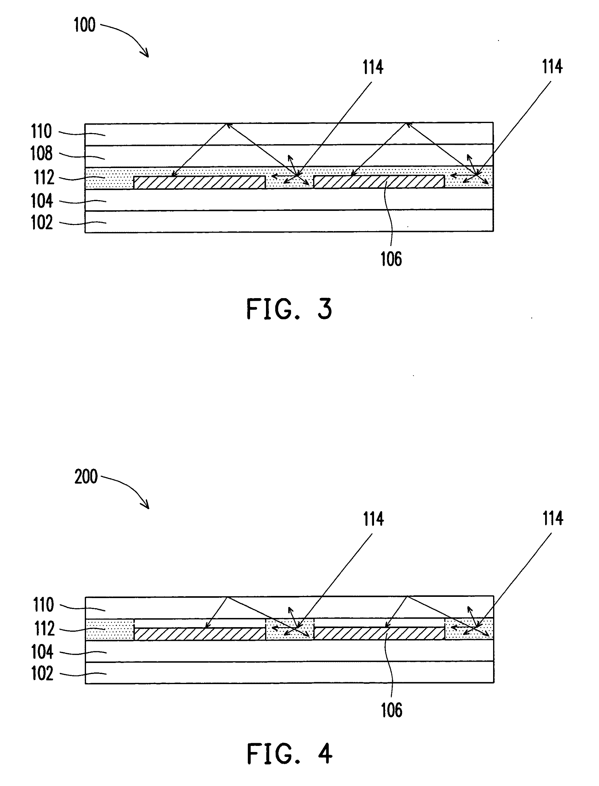
[0057]FIG. 4 is a schematic cross-sectional view showing a crystalline silicon photovoltaic module according to the second embodiment of the present invention. The same reference numerals as those according to the first embodiment are used to represent the same components. According to the second embodiment, a crystalline silicon photovoltaic module 200 includes a first backsheet 102, a first encapsulant layer 104, a plurality of crystalline silicon solar cells 106 and a transparent substrate 110 sequentially stacked. The crystalline silicon photovoltaic module 200 further includes an encapsulant material with porous structure 112 disposed between the crystalline silicon solar cells 106 and between the first encapsulant layer 104 and the transparent substrate 110, thereby replacing the second encapsulant layer according to the first embodiment, so as to collect light passing throughpassing through the crystalline silicon solar cells 106 and to enhance power conversion efficiency of ...

third embodiment

[0058]FIG. 5 is a schematic cross-sectional view showing a crystalline silicon photovoltaic module according to the third embodiment of the present invention. The same reference numerals as those according to the first embodiment are used to represent the same components.

[0059]According to the third embodiment, in a crystalline silicon photovoltaic module 300, a plastic thin film structure 300 is disposed between the crystalline silicon solar cells 106 and between the first encapsulant layer 104 and the second encapsulant layer 108. The plastic thin film structure 300 may be a foamable polymeric material with high glass transition temperatures, and is disposed using an additional stacking method between the crystalline silicon solar cells 106 and between the first encapsulant layer 104 and the second encapsulant layer 108.


PUM

PropertyMeasurementUnit
reflectanceaaaaaaaaaa
light reflectanceaaaaaaaaaa

Abstract

An encapsulant material with enhanced light reflectivity, a crystalline silicon photovoltaic module and a thin film photovoltaic module are provided. The encapsulant material has a porous structure therein, and an average pore diameter of the porous structure is between several hundreds of nanometers and several hundreds of micrometers, so that the light reflectance of the encapsulant material is improved. Moreover, the encapsulant material is crosslinked by a physical or chemical crosslinking method, so heat resistance thereof is improved. Therefore, the encapsulant material is suitable for the crystalline silicon photovoltaic module and the thin film photovoltaic module, so as to increase power conversion efficiency of these modules.

Description

CROSS-REFERENCE TO RELATED APPLICATION[0001]This application claims the priority benefit of Taiwan application serial no. 97148637, filed on Dec. 12, 2008. The entirety of the above-mentioned patent application is hereby incorporated by reference herein and made a part of this specification.BACKGROUND OF THE INVENTION[0002]1. Field of the Invention[0003]The present invention relates to an encapsulant material having enhanced light reflectivity, to a crystalline silicon photovoltaic module and to a thin film photovoltaic module.[0004]2. Description of Related Art[0005]A structure of a photovoltaic module includes a frontsheet, solar cells and a backsheet formed in a laminated sandwiched structure. An encapsulant material therein is mainly used as a barrier layer to protect the solar cells and connecting circuits in the photovoltaic module from environmental hazards like moisture, oxygen, acid rain and salts. A good encapsulant material not only extends life span of the module, but al...

Claims


Application Information

Patent Timeline
Patent Type & Authority Applications(United States)
IPC IPC(8): H01L31/048H01L31/00B32B3/26
CPCB32B17/10009B32B17/1055B32B17/10568H01L31/0547B32B27/16H01L31/048Y02E10/52B32B17/10788B32B3/08B32B27/065B32B27/08B32B27/18B32B27/283B32B27/306B32B27/32B32B27/40B32B2307/202B32B2307/306B32B2307/412B32B2307/416B32B2457/12Y10T428/249978
Inventor HUANG, LEE-MAYPENG, CHENG-YULIANG, WEN-CHUNGCHEN, CHUN-HENG
Owner IND TECH RES INST
Why Eureka
Try Eureka