

Silicon-based thin-film photoelectric conversion device, and method and apparatus for manufacturing the same
a technology of photoelectric conversion device and thin film, which is applied in the direction of sustainable manufacturing/processing, final product manufacturing, coatings, etc., can solve the problems of plurality of flow lines of substrates, increase in solar battery manufacturing cost, and disadvantageous stoppage of entire production lines, etc., to achieve high photoelectric conversion efficiency, excellent quality, and low cost
- Summary
- Abstract
- Description
- Claims
- Application Information
AI Technical Summary
Benefits of technology
Problems solved by technology
Method used
Image

Examples
embodiment 1
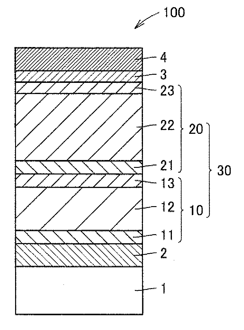
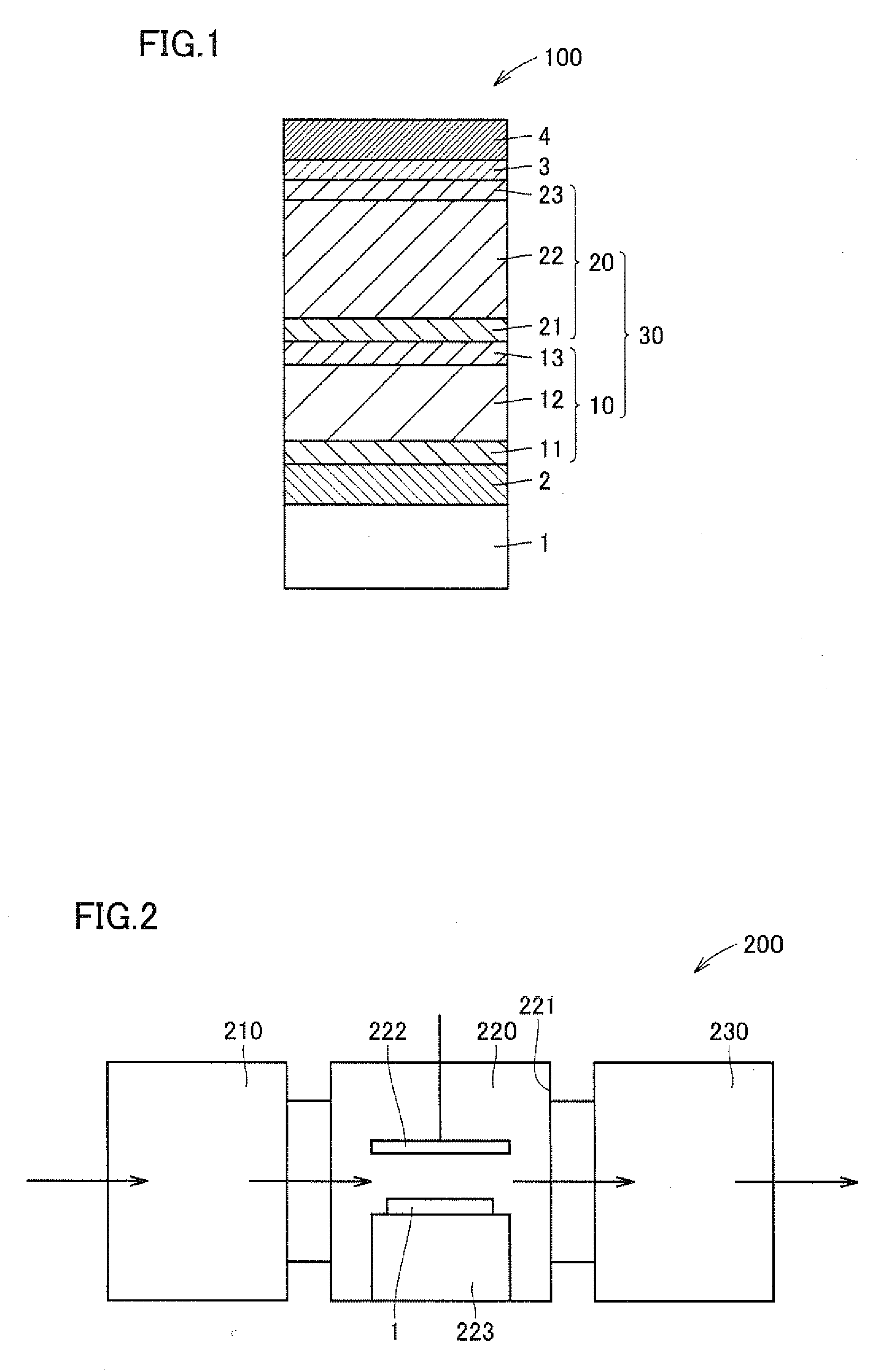
[0036]Referring to FIGS. 1 and 2, one embodiment of the method of manufacturing a silicon-based thin-film photoelectric conversion device according to the present invention is characterized in that the method includes the steps of forming a transparent conductive film 2 on a substrate 1, and forming a double pin structure stack body 30 by successively forming a first p-type semiconductor layer 11, an i-type amorphous silicon-based photoelectric conversion layer 12, a first n-type semiconductor layer 13, a second p-type semiconductor layer 21, an i-type microcrystalline silicon-based photoelectric conversion layer 22, and a second n-type semiconductor layer 23 on transparent conductive film 2, the step of forming double pin structure stack body 30 is performed in an identical plasma CVD film deposition chamber 220, and first p-type semiconductor layer 11, i-type amorphous silicon-based photoelectric conversion layer 12 and first n-type semiconductor layer 13 are formed under such con...
embodiment 2
[0066]Referring to FIGS. 1 and 2, another embodiment of the method of manufacturing a silicon-based thin-film photoelectric conversion device according to the present invention includes the steps of carrying silicon-based thin-film photoelectric conversion device 100 including the double pin structure stack body out of plasma CVD film deposition chamber 220 and removing the remaining film on cathode 222 and / or inner surface 221 in plasma CVD film deposition chamber 220, after the step of forming the double pin structure stack body in Embodiment 1 above. Namely, the method of manufacturing the silicon-based thin-film photoelectric conversion device in the present embodiment is characterized in that, after double pin structure stack body 30 is formed, silicon-based thin-film photoelectric conversion device 100 including double pin structure stack body 30 is carried out of plasma CVD film deposition chamber 220 and the remaining film on cathode 222 and / or inner surface 221 in plasma CV...
embodiment 3
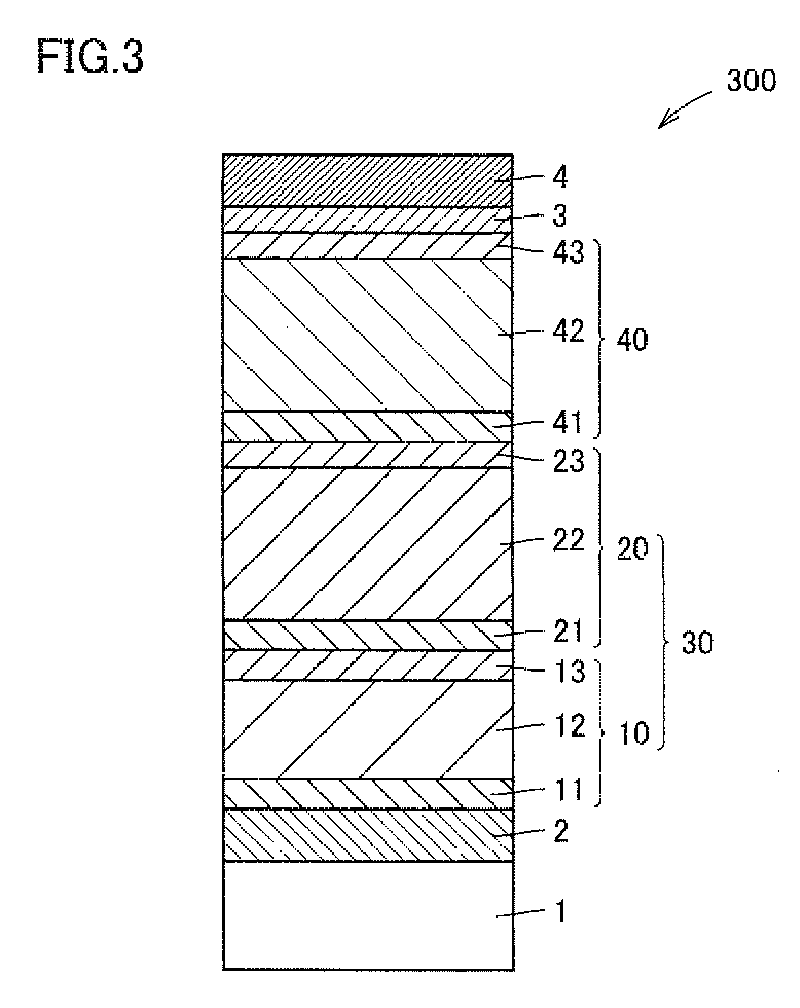
[0079]Referring to FIG. 3, yet another embodiment of the method of manufacturing the silicon-based thin-film photoelectric conversion device according to the present invention is characterized in that at least one crystalline pin structure stack body 40 formed from a p-type semiconductor layer 41, an i-type crystalline silicon-based photoelectric conversion layer 42 and an n-type semiconductor layer 43 is stacked on second n-type semiconductor layer 23 of double pin structure stack body 30 formed with the manufacturing method according to Embodiment 1 or Embodiment 2 above.
[0080]Specifically, referring to FIG. 3, the silicon-based thin-film photoelectric conversion device in the present embodiment is implemented by a stack-type silicon-based thin-film photoelectric conversion device 300 having such a structure that three or more pin structure stack bodies formed from amorphous pin structure stack body 10, microcrystalline pin structure stack body 20 and one or more crystalline pin s...
PUM
| Property | Measurement | Unit |
|---|---|---|
| pressure | aaaaa | aaaaa |
| pressure | aaaaa | aaaaa |
| thickness | aaaaa | aaaaa |
Abstract
Description
Claims
Application Information