Semiconductor device and method for manufacturing the same

a technology of semiconductors and semiconductors, applied in the direction of semiconductor devices, electrical devices, transistors, etc., can solve the problems of difficult control of vsub>th/sub>values to fall within the above range, and achieve the effects of suppressing short-channel effect, low power consumption, and high speed

Inactive Publication Date: 2010-06-24
RENESAS ELECTRONICS CORP
View PDF9 Cites 15 Cited by
  • Summary
  • Abstract
  • Description
  • Claims
  • Application Information

AI Technical Summary

Benefits of technology

[0016]As described above, a semiconductor device including a fully depleted MOS transistor with a metal gate electrode can operate at a low power level and improve mobility (operate at high speed) by lowering the channel dose. Lowering the channel dose, however, disadvantageously makes it difficult to control Vth.
[0035]The present inventor has intensively conducted studies on a variety of metal gate electrode materials and found that NiSi containing a specific impurity may be preferably used as the material that forms the gate electrode of each of the pMOS and nMOS transistors. That is, the present inventor has found that in the thus configured semiconductor device, Vth values of the nMOS and pMOS transistors can be controlled to values necessary for a low-power device and the nMOS and pMOS transistors can be operated at a higher speed, whereby a semiconductor device with excellent device characteristics can be provided.
[0129]It is possible to provide a semiconductor device that consumes low power and can operate at high speed. Specifically, a MOS transistor with a suppressed short-channel effect and improved mobility can be provided by using an SOI structure to reduce parasitic capacitance and substrate leak current and lowering channel dose in the semiconductor region in which a channel region is to be formed.
[0130]Further, using specific materials to form the gate electrodes of the nMOS transistor and the pMOS transistor allows the work functions of the materials that form the gate electrodes to be controlled to desired values. It is therefore possible to provide a semiconductor device with excellent device characteristics in which Vth values of the nMOS transistor and the pMOS transistor are controlled to be desired values.

Problems solved by technology

Lowering the channel dose, however, disadvantageously makes it difficult to control Vth.
Specifically, to achieve a low-power semiconductor device, it is necessary to set Vth of a pMOS transistor to a value ranging from approximately −0.6 to −0.3 V and Vth of an nMOS transistor to a value ranging from approximately 0.3 to 0.6 V. It is, however, very difficult to control the Vth values to fall within the above ranges by using the technology disclosed in Japanese Patent Laid-Open No. 2004-221226.

Method used


Image

  • Semiconductor device and method for manufacturing the same
  • Semiconductor device and method for manufacturing the same
  • Semiconductor device and method for manufacturing the same

Examples


first exemplary embodiment

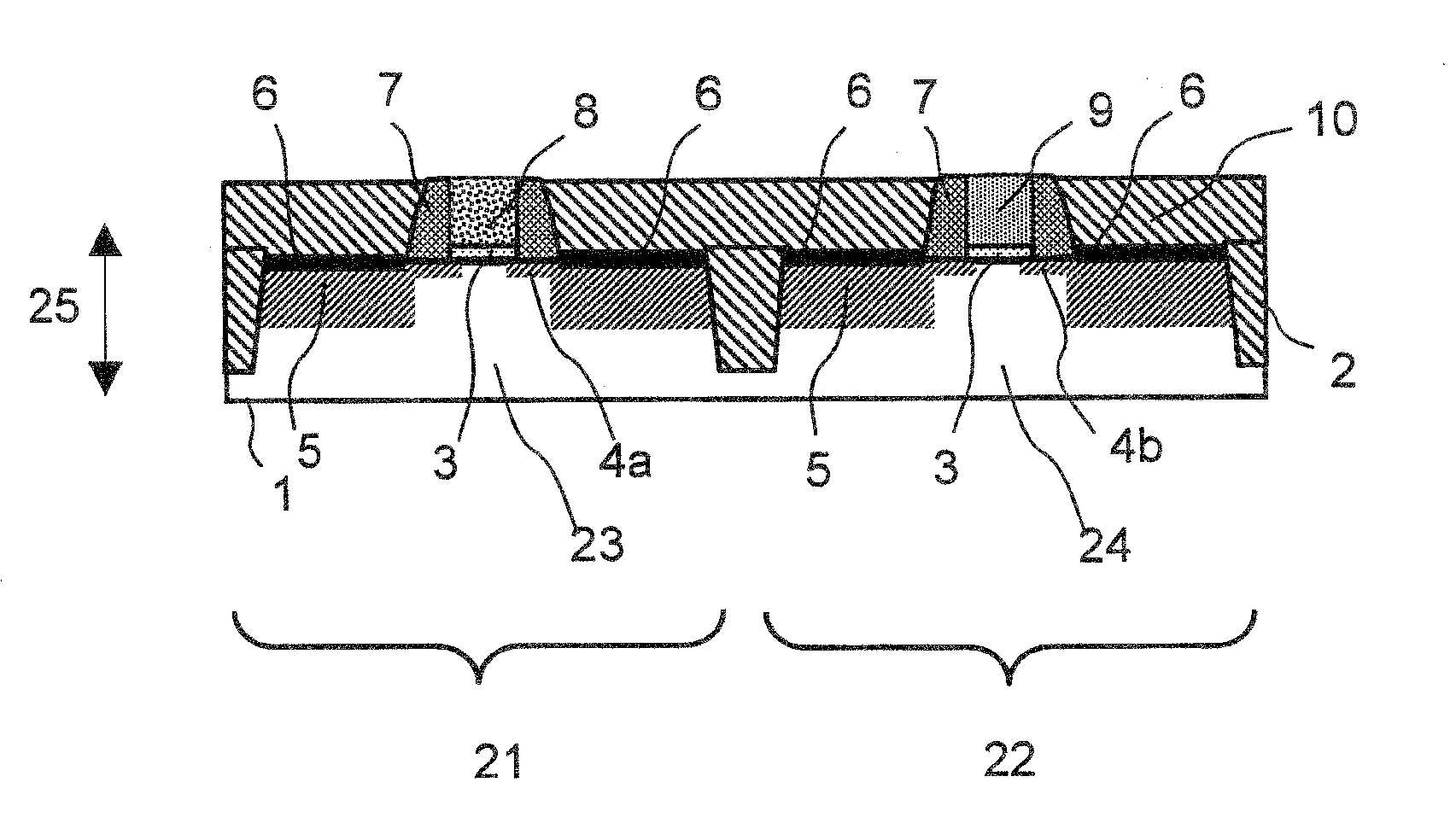
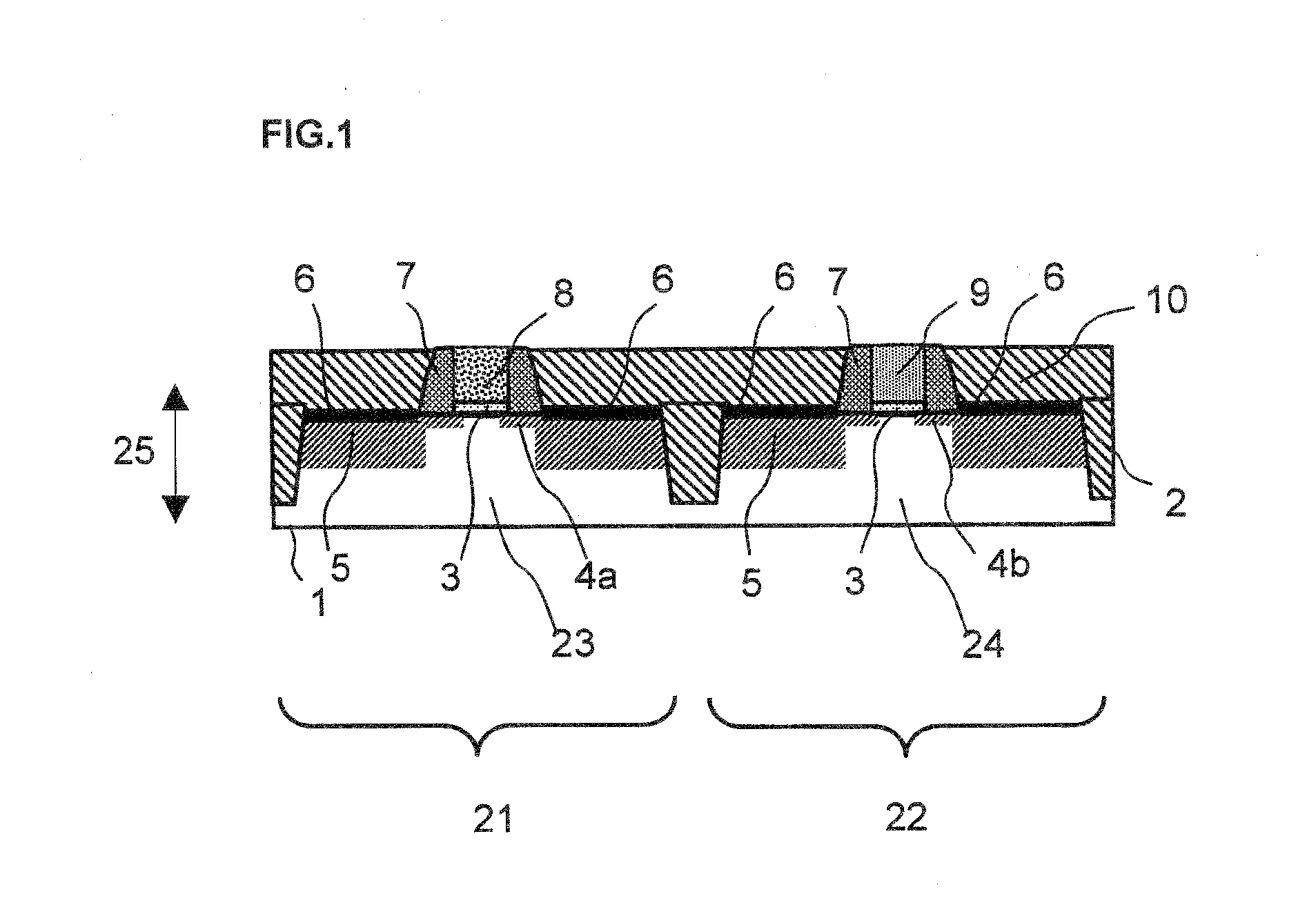
[0208]FIGS. 6 to 9 show an example of a method for manufacturing a semiconductor device of the present invention. FIGS. 6 to 9 show a method for manufacturing a semiconductor device in which each of an nMOS transistor and a pMOS transistor form a planar transistor.

[0209]First, an SOI substrate including support substrate 1, embedded oxide film 11, and a silicon layer with n-type region 24 and p-type region 23 is prepared. The thickness of the silicon layer in the SOI substrate is adjusted in such a way that manufactured MOS transistors are fully depleted. The SOI substrate can be formed by using bonding or SIMOX. For example, a smart-cut method or an ELTRAN method may be used.

[0210]STI (Shallow Trench Isolation) technique is then used to form isolation region 2 in the silicon layer so that n-type region 24 and p-type region 23 are isolated.

[0211]Thermal oxidation is subsequently used to form insulating film 3 comprising a silicon oxynitride film on the surface of the silicon layer. ...

second exemplary embodiment

[0224]FIGS. 13 to 20 explain another example of the method for manufacturing a semiconductor device of the present invention. The manufacturing method relates to a method for manufacturing a semiconductor device including a fin-type MOSFET. First, a substrate with silicon substrate 1, embedded oxide film 11, and silicon semiconductor layer 55 with n-type and p-type regions sequentially stacked is prepared: (FIG. 13(a)).

[0225]Mask pattern 56 is then formed on silicon semiconductor layer 55 (FIG. 13(b)). A silicon oxide film or a silicon nitride film can be used as mask pattern 56, a silicon nitride film is preferably used. Mask pattern 56 is then used as a mask to etch the resulting structure so as to form protruding p-type region 23 and n-type region 24 protruding from embedded oxide film 11 (FIG. 14(a)).

[0226]Thermal oxidation is carried out on p-type region 23 and n-type region 24 to form second gate insulating film 3a and first gate insulating film 3b (SiO2 film) on both sides of...


PUM


Abstract

There is provided a semiconductor device having excellent device characteristics in which Vth values of an nMOS transistor and a pMOS transistor are controlled to be desired values. The semiconductor device includes a pMOS transistor and an nMOS transistor formed by using an SOI substrate. The pMOS transistor is a fully depleted transistor including an n-type region, a first gate electrode, a first gate insulating film, and a source / drain region, and the nMOS transistor is a fully depleted transistor including a p-type region, a second gate electrode, a second gate insulating film, and a source / drain region. The first gate electrode includes silicide region comprising an NiSi crystalline phase containing an n-type impurity, the silicide region being in contact with the first gate insulating film, and the second gate electrode includes silicide region comprising an NiSi crystalline phase containing a p-type impurity, the silicide region being in contact with the second gate insulating film.

Description

TECHNICAL FIELD[0001]The present invention relates to a semiconductor device including a fully depleted nMOS transistor and pMOS transistor formed by using an SOI substrate. The present invention also relates to a low-power semiconductor device in which Vth (threshold voltage) values of the MOS transistors are controlled to exhibit excellent device characteristics.BACKGROUND ART[0002]There has proposed a semiconductor device including an nMOS transistor and a pMOS transistor, each of which includes a metal gate electrode made of a metal or other materials. Such a semiconductor device including a MOS transistor with a metal gate electrode is characterized in that the gate electrode will not be depleted even when the transistor is miniaturized, whereby sufficient drive current (Ion) is provided.[0003]FIG. 1 shows such a semiconductor device. The semiconductor device shown in FIG. 1 includes planar nMOS transistor 21 and pMOS transistor 22. In the semiconductor device, p-type region 23...

Claims


Application Information

Patent Timeline
Patent Type & Authority Applications(United States)
IPC IPC(8): H01L27/092H01L21/8238
CPCH01L21/28097H01L21/823835H01L21/823878H01L21/84H01L21/845H01L29/785H01L27/1211H01L29/4908H01L29/66545H01L29/66803H01L27/1203H01L21/8238H01L27/08H01L27/092H01L29/49
Inventor TAKAHASHI, KENSUKE
Owner RENESAS ELECTRONICS CORP
Why Eureka
Try Eureka