Electrophotographic photosensitive body, method for producing conductive base, image forming device, and electrophotographic cartridge

a photosensitive body and electrophotography technology, applied in the direction of electrographic process equipment, optics, instruments, etc., can solve the problems of interference fringe, uneven image formation of photoreceptors, and various defects of photoreceptors, and achieve high performance

Inactive Publication Date: 2010-06-24
MITSUBISHI CHEM CORP
View PDF7 Cites 12 Cited by
  • Summary
  • Abstract
  • Description
  • Claims
  • Application Information

AI Technical Summary

Benefits of technology

[0034]The present invention can provide an electrophotographic photoreceptor achieving high performance that hardly generates image defects such as black spots, color spots, and interference fringes, a process of producing an electroconductive substrate to be used in the electrophotographic photoreceptor, and an image-forming apparatus and an electrophotographic cartridge that include the photoreceptor.

Problems solved by technology

In the organic photoreceptor, changes in use environment of the photoreceptor or changes in electric characteristics during repeated use may cause various defects in an image formed with the photoreceptor.
However, an image formed with a photoreceptor has unevenness, a so-called interference fringe, as one of the image defects.
This causes unevenness in intensity of light that affects a charge-generating layer, resulting in irregular sensitivities at different positions over the area.

Method used


Image

  • Electrophotographic photosensitive body, method for producing conductive base, image forming device, and electrophotographic cartridge
  • Electrophotographic photosensitive body, method for producing conductive base, image forming device, and electrophotographic cartridge
  • Electrophotographic photosensitive body, method for producing conductive base, image forming device, and electrophotographic cartridge

Examples


example 1

[Substrate 1]

[0399]A substrate 1 made of an aluminum alloy A6063 defined in JIS H4040 and having an outer diameter of 30 mm, a length of 357 mm, and a thickness of 1.0 mm was prepared by cutting with a polycrystalline diamond bit such that the maximum height surface roughness Rz was 1.3 μm. Part of the substrate 1 was used for measurement of the in-plane arithmetic mean roughness Ra, the maximum height surface roughness Rz, and the kurtosis Rku of the substrate 1. Specifically, these values were measured according to JIS B0601:1994 with a surface roughness measuring instrument “Surfcom 480A”, manufactured by Tokyo Seimitsu Co., Ltd., and the obtained values were applied to the specification of JIS B0601:2001. The results are shown in Table 3.

[Coating Liquid for Undercoat Layer]

[0400]Surface-treated titanium oxide was prepared by mixing rutile titanium oxide having an average primary particle diameter of 40 nm (“TTO55N”, manufactured by Ishihara Sangyo Co., Ltd.) and methyldimethoxys...

example 2

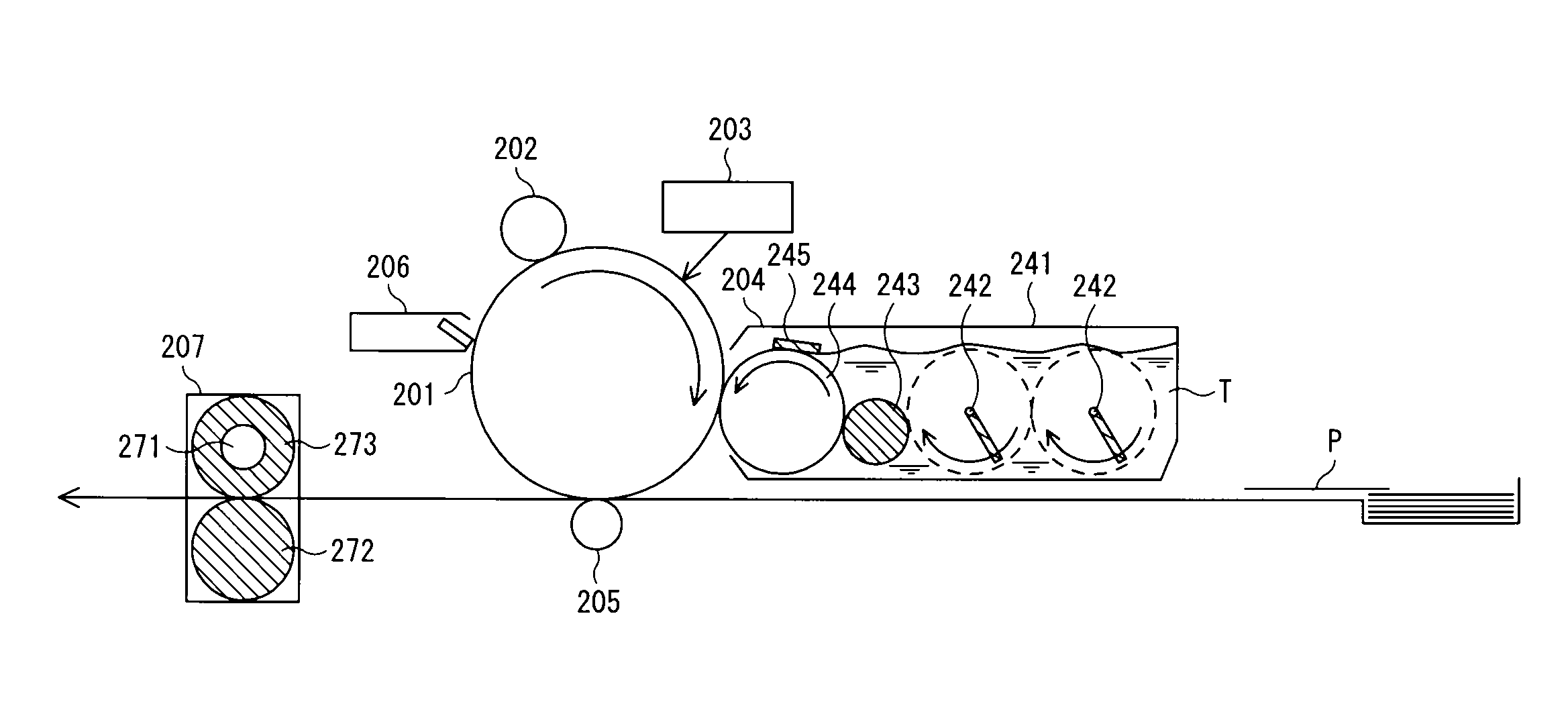
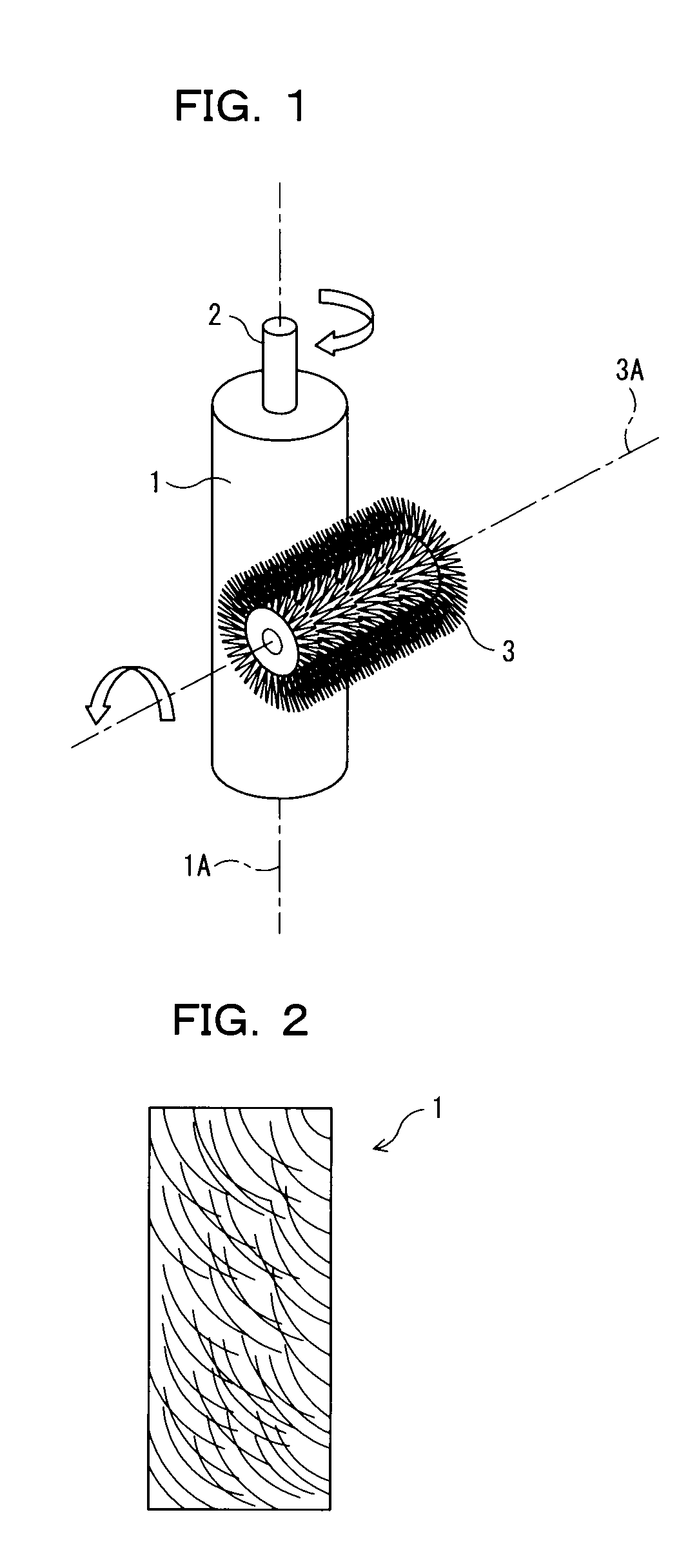
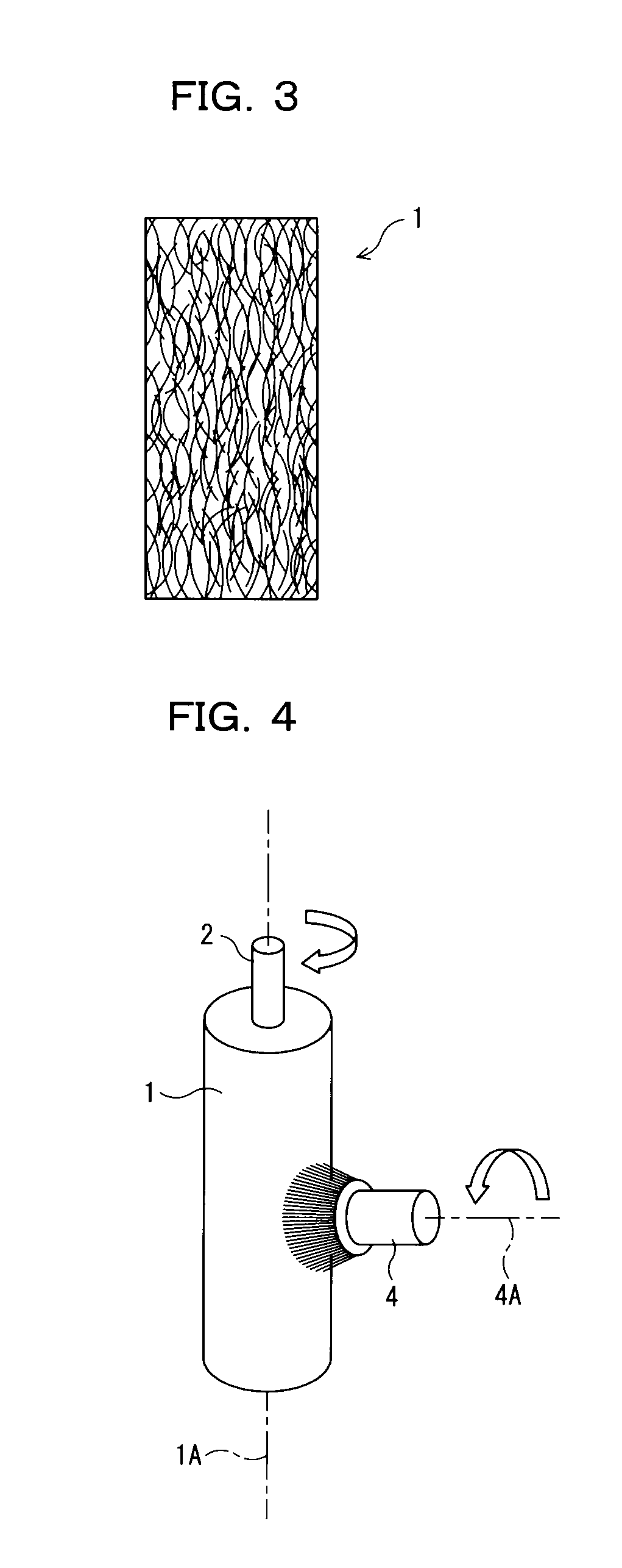
[0408]A mirror-finished cut tube (Ra: 0.03, Rz: 0.2) (sic) of an aluminum alloy A6063 defined in JIS H4040 and having an outer diameter of 30 mm, a length of 357 mm, and a thickness of 1.0 mm was subjected to a roughening process using a brush composed of a cylindrical bed of PVC having an outer diameter of 60 mm and being provided with holes having a hole diameter of 5 mm in a zigzag array at 10-mm intervals and a nylon material (“Tynex A”, manufactured by Dupont), containing alumina abrasive grains having a diameter of 0.45 mm and a grain size #500 (average grain diameter: 34 μm), planted in the holes so as to have a length of 25 mm. The roughening was conducted by rotating the substrate at a rotational speed of 200 rpm and rotating the brush at a rotational speed of 750 rpm, with a contact width of 10 mm, a pulling-up speed of 5 mm / sec, and a sprinkling water volume of 1 L / min. The pulling-up speed was set as high as possible within the range that does not cause a low groove dens...

example 3

[0413]An ironed tube of an aluminum alloy A3003 defined in JIS H4040 and having an outer diameter of 30 mm, a length of 357 mm, and a thickness of 1.0 mm was subjected to a roughening process as in Example 2 to obtain a substrate 3.

[0414]A part of the resulting substrate 3 was put aside for measurement of the surface roughness and the groove width. The remaining washed substrate 3 was provided with a photosensitive layer as in Example 1 to give a photoreceptor P3.

[0415]An image was formed using the resulting photoreceptor P3 as in Example 1 and was evaluated by visual inspection. The results are shown in Table 3.

[0416]The substrate 3 put aside was subjected to measurement of the in-plane arithmetic mean roughness Ra, the maximum height surface roughness Rz, and the kurtosis Rku as in Example 2. Furthermore, the maximum value (maximum lateral width) and the minimum value (minimum lateral width) of groove width L of the grooves formed on the surface of the substrate 3 were measured. T...


PUM

PropertyMeasurementUnit
particle diameteraaaaaaaaaa
weight ratioaaaaaaaaaa

Abstract

An electrophotographic photoreceptor having high performance that hardly generates image defects such as black spots, color spots, and interference fringes is provided. The electrophotographic photoreceptor includes an undercoat layer containing metal oxide particles and a binder resin on an electroconductive substrate having a maximum height surface roughness Rz in the range of 0.8≦Rz≦2 μm, and a photosensitive layer disposed on the undercoat layer, wherein the metal oxide particles have a volume average particle diameter of 0.1 μm or less and a 90% cumulative particle diameter of 0.3 μm or less which are measured by a dynamic light-scattering method in a liquid containing the undercoat layer dispersed in a solvent mixture of methanol and 1-propanol at a weight ratio of 7:3.

Description

TECHNICAL FIELD [0001]The present invention relates to an electrophotographic photoreceptor, a process of producing an electroconductive substrate to be used in the photoreceptor, and an image-forming apparatus and an electrophotographic cartridge that include the photoreceptor.BACKGROUND ART [0002]Electrophotographic technology has been widely applied to the field of various printers, recently, as well as the field of copiers, due to its immediacy and formation of high-quality images. Electrophotographic photoreceptors (hereinafter, optionally, referred to as “photoreceptor”) lie in the core technology of electrophotography, and organic photoreceptors using organic photoconductive materials have been developed, since they have advantages such as non-pollution and ease in production in comparison with inorganic photoconductive materials.[0003]In general, an organic photoreceptor is composed of an electroconductive substrate and a photosensitive layer disposed thereon. Photoreceptors...

Claims


Application Information

Patent Timeline
Patent Type & Authority Applications(United States)
IPC IPC(8): G03G21/16G03G5/14G03G15/00
CPCG03G5/10G03G15/75G03G5/144G03G5/0564G03G5/0616
Inventor MITSUMORI, TERUYUKIISHIO, KOZOFUCHIGAMI, HIROETAGUCHI, SUSUMUKURIHARA, SHUNICHIRO
Owner MITSUBISHI CHEM CORP
Why Eureka
Try Eureka