Flash memory device and manufacturing method of the same

a technology of flash memory and manufacturing method, which is applied in the direction of semiconductor devices, basic electric elements, electrical apparatus, etc., can solve the problems of unsuitable mobile product recovery operation, unnecessarily required recovery operation, and inability to meet the requirements of mobile product storage, etc., to achieve the effect of reducing the number of high voltage devices, and reducing the area of the peripheral region

Inactive Publication Date: 2010-07-01
DONGBU HITEK CO LTD
View PDF5 Cites 11 Cited by
  • Summary
  • Abstract
  • Description
  • Claims
  • Application Information

AI Technical Summary

Benefits of technology

[0015]In addition, an embodiment has a 2-Tr structure, so the over-erase problem caused by a select gate can be basically prevented. Thus, unnecessary circuits and unnecessary operations, such as a recovery operation or an iteration operation for preventing the over-erase, may not be required. In addition, since the flash memory device of an embodiment has a high coupling ratio, the program / erase operations can be performed under relatively low bias and low voltage, so that the number of high voltage devices, high voltage driving circuits, and high voltage pumping circuits can be reduced. Therefore, the area of the peripheral region can be significantly reduced.
[0016]Further, an embodiment provides a flash memory device and a method for manufacturing the same, which can significantly reduce the cell size as compared with a flash memory having the 2-Tr structure according to the related art, and can significantly reduce an area of a cell peripheral region because the flash memory has the higher coupling ratio as compared with that of the flash memory having the 1-Tr ETOX structure.
[0017]In addition, an embodiment provides a flash memory device and a method for manufacturing the same, in which a select gate structure is defined as a self-align structure, so that a length of a select gate is controlled depending on a thickness of the select gate rather than photo and etch processes, thereby ensuring the length of the select gate.

Problems solved by technology

In addition, a tunnel oxide layer must have thin thickness of 20 to 30 Å, so the FN tunneling scheme has a disadvantage in terms of data retention.
In contrast, the channel hot electron injection scheme has an advantage of high speed programming of few μs, but high current of several hundreds of μA is required for cell programming, so the channel hot electron injection scheme is not suitable for mobile products due to its high power consumption.
In addition, if a cell having a 1-Tr structure is used, over-erase may occur during the erase operation, so the recovery operation is unnecessarily required.
Further, for the 2-Tr structure memory cell device, the cell size is significantly enlarged and the manufacturing process is complicated.
In addition, due to the low coupling ratio, high bias is required.
Further, similar to the design of FIG. 1A, the coupling ratio is low and complicated circuits or applications are necessary to solve problems such as over-erase or over program.

Method used


Image

  • Flash memory device and manufacturing method of the same
  • Flash memory device and manufacturing method of the same
  • Flash memory device and manufacturing method of the same

Examples


first embodiment

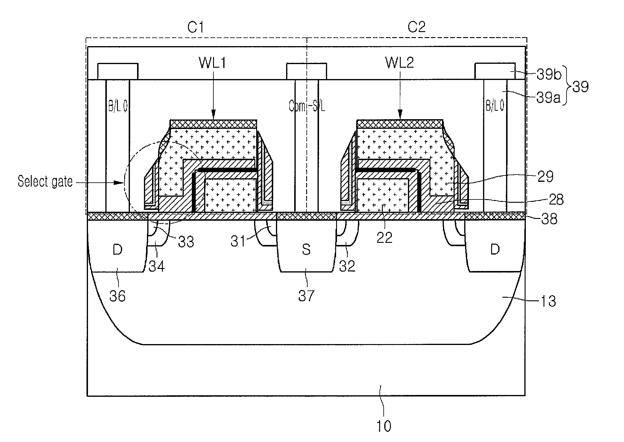
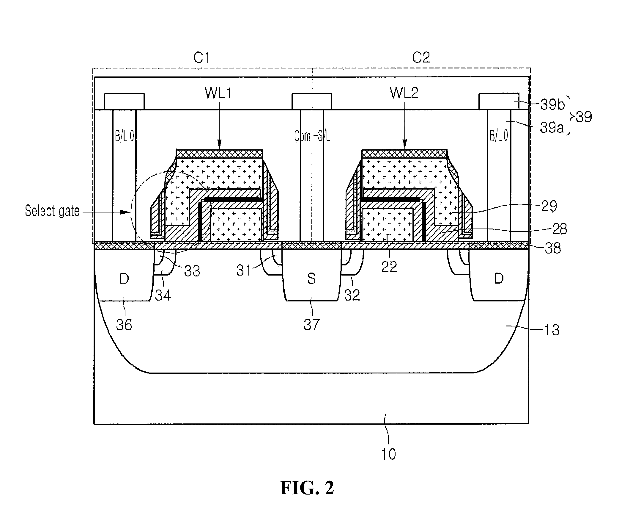
[0032]Hereinafter, the operation of the flash memory device will be described with reference to FIGS. 2 and 3A to 3C, and Table 1. FIG. 2 shows a cross-sectional view through line A-A′ of FIG. 3A in accordance with an embodiment of the invention. As illustrated by the schematic diagram of FIG. 3A, each cell includes the two transistor configuration of select gate and floating gate, and the cells are configured in pairs of adjacent cells. The small size can be accomplished by using the split select gate and floating gate configuration of embodiments of the invention to provide the adjacent cell pairs.

[0033]A sector is defined by using divided high voltage p-wells (HPWs). The HPWs are isolated from each other by deep n-wells (DNWs). Each HPW can be applied with a signal IPW0> to IPW. For one embodiment, such as shown in FIG. 3A, a plurality of cells across multiple bit lines and multiple word lines can be included in one sector. Therefore, as described in more detail below, erase ope...

second embodiment

[0043]Hereinafter, the operation of the flash memory device will be described with reference to FIGS. 2 and 4A to 4C, and Table 2.

[0044]FIG. 2 can represent a cross-sectional view through line A-A′ of FIG. 4A in accordance with an embodiment of the invention. As illustrated by the schematic diagram of FIG. 4A, each cell includes the two transistor configuration of select gate and floating gate, and the cells are configured in pairs of adjacent cells. The small size can be accomplished by using the split select gate and floating gate configuration of embodiments of the invention to provide the adjacent cell pairs.

[0045]A sector is defined by using divided HPWs. The HPWs are isolated from each other by DNWs. Each HPW can be applied with a signal IPW0> to IPW. For one embodiment, such as shown in FIG. 4A, a plurality of cells across multiple word lines can be included in one sector. This can be accomplished using isolated HPWs that are prepared perpendicularly to the word lines W / L. F...


PUM


Abstract

Disclosed are a flash memory device and a method for manufacturing the same. The flash memory device includes a floating gate including adjacent first and second floating gates on a substrate; first and second select gates respectively on the first and second floating gates; an insulating layer between the first floating gate and the first select gate and between the second floating gate and the second select gate; a drain region at outer sides of the first and second select gates; a source region between the first and second select gates; and a metal contact on each of the drain region and the source region. The select gate can be defined as a self-align structure, and the length of the select gate can be controlled depending on the thickness of the material used to form the select gate.

Description

CROSS-REFERENCE TO RELATED APPLICATION[0001]This application claims the benefit under 35 U.S.C. §119 of Korean Patent Application No. 10-2008-0138891, filed Dec. 31, 2008, which is hereby incorporated by reference in its entirety.BACKGROUND[0002]A flash memory device is a nonvolatile memory device that does not lose data stored therein even if power is turned off. In addition, the flash memory can record, read, and delete data at a relatively high speed.[0003]Accordingly, the flash memory device is widely used for the Bios of a personal computer (PC), a set-top box, a printer, and a network server in order to store data. Recently, the flash memory device is extensively used for digital cameras and portable phones.[0004]In such a flash memory device, a stack gate type semiconductor device employing a floating gate and a semiconductor device having a SONOS (Silicon-Oxide-Nitride-Oxide-Silicon) structure are mainly used.[0005]Electron injection schemes for a memory cell of a flash memo...

Claims


Application Information

Patent Timeline
Patent Type & Authority Applications(United States)
IPC IPC(8): H01L29/792H01L21/336
CPCH01L21/28273H01L27/11521H01L29/42328H01L29/66825H01L29/7781H01L29/7881H01L29/40114H10B41/30H01L21/265H10B41/35
Inventor KWON, YOUNG JUN
Owner DONGBU HITEK CO LTD
Why Eureka
Try Eureka